Owing to weak light-matter interactions in natural materials, it is difficult to dynamically tune and switch emission polarization states of plasmonic emitters (or antennas) at nanometer scales. Here, by using a control laser beam to induce a bubble (n=1.0) in water (n=1.333) to obtain a large index variation as high as |Δn|=0.333, the emission polarization of an ultra-small plasmonic emitter (~0.4λ2) is experimentally switched at nanometer scales. The plasmonic emitter consists of two orthogonal subwavelength metallic nanogroove antennas on a metal surface, and the separation of the two antennas is only sx=120 nm. The emission polarization state of the plasmonic emitter is related to the phase difference between the emission light from the two antennas. Because of a large refractive index variation (|Δn|=0.333), the phase difference is greatly changed when a microbubble emerges in water under a low-intensity control laser. As a result, the emission polarization of the ultra-small plasmonic emitter is dynamically switched from an elliptical polarization state to a linear polarization state, and the change of the degree of linear polarization is as high as Δγ≈0.66. Owing to weak light-matter interactions in natural materials, it is difficult to dynamically tune and switch emission polarization states of plasmonic emitters (or antennas) at nanometer scales. Here, by using a control laser beam to induce a bubble (n=1.0) in water (n=1.333) to obtain a large index variation as high as |Δn|=0.333, the emission polarization of an ultra-small plasmonic emitter (~0.4λ2) is experimentally switched at nanometer scales. The plasmonic emitter consists of two orthogonal subwavelength metallic nanogroove antennas on a metal surface, and the separation of the two antennas is only sx=120 nm. The emission polarization state of the plasmonic emitter is related to the phase difference between the emission light from the two antennas. Because of a large refractive index variation (|Δn|=0.333), the phase difference is greatly changed when a microbubble emerges in water under a low-intensity control laser. As a result, the emission polarization of the ultra-small plasmonic emitter is dynamically switched from an elliptical polarization state to a linear polarization state, and the change of the degree of linear polarization is as high as Δγ≈0.66.
Introduction
Surface plasmon polaritons (SPPs) with subwavelength field confinements can significantly shrink the sizes of photonic devices and improve integration densities of photonic integrated circuits1-5. However, the inherent Ohmic loss in metallic nanostructures is a major obstacle, limiting the practical applications of plasmonic devices6-9. Ultra-compact plasmonic emitters and receivers, which are an analog of microwave and radio-wave emitters and receivers, can be used to realize inter-chip optical communications between different photonic devices and different photonic chips10-15. By using inter-chip optical communications, the obstacle of the inherent Ohmic loss in metallic nanostructures can be overcome13, 15.
Up to now, a variety of plasmonic antennas were proposed to realize plasmonic emitters and receivers, including nanorod antennas16, 17, slot antennas18-20, V- (or U-) shaped antennas21, 22, Yagi-Uda antennas23-25, and so on. Most of these plasmonic antennas18, 21-24 were designed to control emission directions, greatly increasing the collection efficiencies of these plasmonic emitters. Recently, some works proposed to design plasmonic antennas to tailor emission polarization states, which provided new degrees of freedom in information encoding and increased communication capacity in inter-chip optical communications26. For example, by using Au nanoparticle antennas, the emission polarization of a dipole located at the antennas was tailored in theory27. By designing an orthogonal elongated nanorod and complementary nanoslit antennas, the polarization control of free-space incident light was theoretically predicted28. By designing a metallic nanogroove antenna with a tilted angle on a gold film, emission light coming from an SPP waveguide mode was rotated in experiments13. Recently, Chen’s group designed metasurface-based emitters on a two-dimensional plasmonic ridge waveguide, and the emission polarization of these metasurface-based emitters was experimentally tailored in both spectral and spatial domains at will15.
Because of subwavelength field confinements of plasmonic antennas, the sizes of these plasmonic emitters were smaller than wavelengths. These subwavelength plasmonic emitters could significantly increase the integration densities of photonic chips15. However, in such a small device size (<0.6λ2), it is difficult to dynamically tune and switch the emission polarization of these ultra-small plasmonic emitters owing to weak light-matter interactions in natural materials29-34 and short interaction lengths ( ≤ device size). Herein, λ is a vacuum wavelength. As far as we know, polarization-switchable plasmonic emitters at nanometer scales have not been reported. Usually, to obtain large dynamic tuning ranges in active plasmonic devices30-34, a large device size was required. For example, to efficiently switching (or modulating) optical signals, the sizes of plasmonic switchers (or modulators) were greater than 10 μm by using electro-optical33, 34, magneto-optical32, and all-optical30 methods. Therefore, it is still a great challenge to efficiently tune and switch the emission polarization of ultra-small plasmonic emitters at nanometer scales.
Design and principle
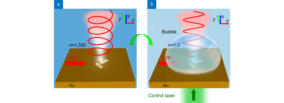
In the letter, we propose to use a control laser to induce a bubble in water to dynamically switch the emission polarization of an ultra-small plasmonic emitter at nanometer scales. Under a low control intensity, an index variation brought about by the laser-induced bubble effect can reach up to 0.3334, 35, 36. This index variation is much greater than those (|Δn|≤0.06) induced by electro-optical33, 34, 37, 38, thermo-optical39, 40, magneto-optical32, 41, and all-optical 29, 42-44 tuning methods. Our designed plasmonic emitter (size ~0.4λ2) consists of two orthogonal subwavelength metallic nanogroove antennas on a metal surface, and the separation of the two antennas is only sx=120 nm. The ultra-small plasmonic emitter exhibits two different emission polarization states (linear polarization state and circular polarization state) when the plasmonic emitter is covered by different media with refractive indices of n=1.333 and 1.0. By using a control laser beam to induce a bubble (n=1.0) in water (n=1.333)4, 35, 36, the emission polarization of the plasmonic emitter is dynamically switched from an elliptical polarization state to a linear polarization state in experiments.
The polarization-switching emitter consists of two orthogonal subwavelength metallic nanogroove antennas on a metal surface, as shown in Fig. 1(a). The metal surface is covered by a medium with a refractive index of n. An SPP mode confined on the metal surface propagates along the x-axis, and it then excites the resonant mode in the nanogroove antenna under a resonant condition13. Our previous works show that the emission polarization from the nanogroove antenna can be rotated by tilting the angle of the nanogroove antenna13, 15. For two orthogonal nanogroove antennas on the metal surface (Fig. 1(a)), the polarization orientations of the emission light from the two nanogroove antennas are orthogonal13. The powers of the emission light from the two antennas can be adjusted by the structural parameters of the two antennas13, 15. The phase difference (φ) of the emission light from the two antennas can be written as15
Figure 1.(a) Circularly polarized emission light as the plasmonic emitter is covered by water (n=1.333). (b) Linearly polarized emission light as the plasmonic emitter is covered by a bubble (n=1.0) induced with a control laser beam.
where k0=2π/λ is a vacuum wave-vector;neff(n)=[εmetal×n2/(εAu+n2)]1/2 is the effective refractive index of the SPP mode confined on the metal surface, and it is sensitive to the refractive index (n) of the surrounding medium29, 35; εmetal is a relative permittivity of metal; φ1 and φ2 are the scattering phases of the two antennas, respectively; φt is the phase propagating through the first antenna; sx is the separation of the two nanogroove antennas along the x-axis. The emission polarization state of the plasmonic emitter is determined by the value of φ. For φ=π/2+mπ (m being an integer), the emission light is circularly polarized (Fig. 1(a)). When the phase difference is changed to be φ=m'π (m' being an integer), the emission light is switched to be linearly polarized (Fig. 1(b)). Hence, the emission polarization state from the plasmonic emitter (Fig. 1(a)) can be switched by changing the refractive index (n) of the covered medium on the metal surface, as shown in Fig. 1. To realize this polarization-switching phenomenon, the smallest phase change is Δφ=π/2. For an ultra-small plasmonic emitter with sx < λ, a large index variation (Δn>0.25) is need to obtain Δφ=π/2 based on Eq. (1). The smaller the device size (sx) is, the larger the index variation (Δn) is required. Such a large index variation is difficult to be achieved by using electro-optical33, 34, 37, 38, thermo-optical39, 40, magneto-optical32, 41, and all-optical29, 42-44 tuning methods. Herein, we propose to use a control laser to induce a bubble (n=1.0) in water (n=1.333)35, and a large index variation as high as Δn=0.333 is obtain to realize efficient polarization switching.
Simulation and discussion
To validate that this large index variation (Δn=0.333) can realize polarization switching in our designed plasmonic emitter, the properties of the emission light from one nanogroove antenna covered by different mediums with refractive indices of n=1.333 and n=1.0 are first studied by employing the finite element method of Comsol Multiphysics. The schematic of a nanogroove antenna is displayed in Fig. 2(a). The length, width, depth, and tilting angle of the nanogroove are l, w, d, and θ, respectively. In simulations, the metal film is set as gold, and its relative permittivity is εAu=−32.78+2.00i at a vacuum wavelength of λ=900 nm45. By varying the tilting angle of the nanogroove antenna, the properties (power, polarization orientation angle, and degree of linear polarization)13, 15 of the emission light from the nanogroove antenna are calculated at λ=900 nm when n=1.0 (black lines) or n=1.333 (red lines), as displayed in Fig. 2(b–d). The simulation method and the definition of the polarization orientation angle and degree of linear polarization can be found in our previous works13, 15. Here, the length, width, and depth of the nanogroove are fixed to be l=400 nm,w=100 nm, and d=200 nm, respectively. Further simulation results show that the resonant wavelengths of the antenna covered by different mediums with refractive indices of n=1.333 and n=1.0 are λ'≈970 nm and λ''≈880 nm, respectively. Similar resonant spectra of the nanogroove antenna can be found in our previous works13, 15. Hence, the difference of the powers of the emission light from the nanogroove antenna covered by a medium with a refractive index of n=1.0 and a medium with a refractive index of n=1.333 at the working wavelength λ=900 nm is small, as shown in Fig. 2(b). By slightly adjusting the working wavelength or structural parameters of the nanogroove antenna, the power difference can become smaller.
Figure 2.(a) Structure diagram and geometry parameters of a nanogroove antenna. Simulated (b) powers, (c) polarization orientation angles, and (d) degrees of linear polarization (Dp) of the emission lights from one nanogroove antenna when the antenna is covered by different mediums with refractive indices of n=1.333 (red lines) and n=1.0 (black lines).
For θ<50°, the polarization orientation angles of the emission light from the antenna covered by a medium with a refractive index ofn=1.0 are approximately equal to that covered by a medium with a refractive index of n=1.333, as shown in Fig. 2(c). The reason is that the polarization orientation angle of the emission light is mainly determined by the tilting angle of the antenna13. For θ=45°, the polarization orientation angles of the emission light from the antenna covered by different mediums with refractive indices of n=1.333 and n=1.0 are both approximately α=45°. Moreover, the degrees of linear polarization (γ)13, 15 of the emission light from the antenna covered by different mediums with refractive indices of n=1.333 and n=1.0 are nearly the same, and they are both greater than 0.9 for θ<50°, as shown inFig. 2(d). This indicates that the degrees of linear polarization of the emission light from the nanogroove antenna remain high for n=1.333 and n=1.0.
The above simulations show that the refractive index of the covered medium (n=1.333 or n=1.0) has little influence on the polarization orientation angle and degree of linear polarization of the emission light from the nanogroove antenna. Based on Eq. (1), the refractive index of the covered medium (n=1.333 or n=1.0) has large influence on the phase difference (φ) of the emission light from the two antennas in Fig. 1. To test our analysis, the polarization states of the plasmonic emitter (Fig. 3(a)) covered by different mediums with refractive indices of n=1.333 and n=1.0 are simulated. Figure 3(a) shows the top view of the two orthogonal subwavelength metallic nanogroove antennas (θ1=45° and θ2=−45°) as well as the structural parameters. When the structural parameters are l=400 nm,w=100 nm, d1=200 nm, d2=180 nm, sy=300 nm, and sx=120 nm, the simulation results of the polarization states of the emission light are displayed in Fig. 3(b, c). It is observed that the emission light from the plasmonic emitter is circularly polarized for n=1.333, as shown by the red line in Fig. 3(b). The degrees of linear polarization is calculated to be γ=0.03 (Fig. 3(c)). When the refractive index of the covered medium is changed to be n=1.0, the emission light from the plasmonic emitter turns to be linearly polarized, as shown by the black line in Fig. 3(b). In this case, the degrees of linear polarization is calculated to be γ'=0.74 (Fig. 3(c)). The polarization orientation angle of the linearly polarized emission light from the plasmonic emitter is αair≈350°. The reason is that the intensity of the emission light from the upper nanogroove antenna is greater than that from the lower nanogroove antenna. Hence, by changing the refractive index of the covered medium from n=1.333 to n=1.0, the emission polarization of the plasmonic emitter is switched from near-circular polarization to near-linear polarization (|Δγ|>0.5) in a wavelength range fromλ=870 nm to λ=980 nm, as shown in Fig. 3(c).
Figure 3.(a) Structure diagram and geometry parameters of the plasmonic emitter. (b) Polar plot of the simulated intensity of the emission light from the plasmonic emitter as a function of the polarization angle for n=1.333 (red line) or n=1.0 (black line) at λ=900 nm. (c) Degrees of linear polarization of the emission light from the plasmonic emitter varying with the wavelengths for n=1.333 (red line) or n=1.0 (black line).
To test our proposal experimentally, the plasmonic emitter consisting of two nanogroove antennas is fabricated by a focused ion beams (FIB) method on a 450 nm thick gold film, which is deposited on a glass substrate with a 30 nm thick titanium adhesion layer13. Here, three plasmonic emitters with the same geometrical parameters are fabricated in a column with a separation of about 5 μm, as shown on the right side of Fig. 4(a). A slit with a length of 20 μm and a width of 100 nm is fabricated on the gold film to excite the SPP mode on the front gold surface under the back-side illumination46, as shown by the left side of Fig. 4(a). The separation of the slit and plasmonic emitters is 15 μm. The zoomed-in scanning electron microscope (SEM) image of the plasmonic emitter is displayed in Fig. 4(b), and the cross-section of the nanogroove antenna is shown in Fig. 4(c). It is observed that the nanogroove tapers down to the bottom because of the fabrication limit of the FIB method. This deviation affects the resonant wavelength, but it has little influence on the polarization orientation angle and degree of linear polarization of the emission light from the nanogroove antenna. The measured geometrical parameters of the two nanogroove antennas are l≈400 nm,w≈100 nm, d1≈220 nm, d2≈160 nm, sy≈300 nm, and sx≈120 nm.
Figure 4.(a) SEM image of the fabricated structure. (b) Zoomed-in SEM image of a plasmonic emitter. (c) Cross-section of a nanogroove antenna. The green lines is used to measure the thickness of the gold film and the depth of the nanogroove antenna. (d) Schematic of the measurement set-up.
Then, a 25 mm×25 mm cover glass is placed above the gold film to form a gap. We drop water into the gap and press the cover glass to get a thin water film (about 10 μm). The samples are measured by using a home-built microscopy imaging system, as shown in Fig. 4(d). A p-polarized monochromatic light with a wavelength of λ (red beam in Fig. 4(d)) is focused on the substrate by a microscope objective (Mitutoyo 20× and NA=0.4). The SPP mode on the front metal surface is excited and then impinges the plasmonic emitters. The emission light from the plasmonic emitters is collected by another objective (Mitutoyo 100× and NA=0.5). After passing a long-pass filter (cut-off wavelength=600 nm) and a polarizer, the emission light is imaged onto a complementary metal-oxide-semiconductor transistor (CMOS). A control laser beam (green beam in Fig. 4(d)) with a wavelength of λc=532 nm is also focused on the structure from the backside. The gold film absorbs the control laser, and the water on the water-gold interface is heated, inducing a bubble under a critical intensity of the control laser beam. A white light-emitting diode (LED) illuminates the structure from the front side to monitor the bubble emerging on the gold surface. The long-pass filter (600 nm) is used to block the pump light, and the polarizer is used to collect CMOS images at different polarizer angles.
The polarization states of the emission light from the plasmonic emitter are investigated when the plasmonic emitter is covered by air or water (without the control light). When the plasmonic emitter is covered by air (n=1.0), the captured CMOS image is displayed in Fig. 5(a) (at an incident wavelength of λ=900 nm). It is observed that there are three bright spots on the right side of Fig. 4(a), which indicates that the confined SPP mode is emitted into the free-radiation field by the plasmonic emitters. The left bright line is the directly transmitted light from the 100-nm-wide slit. By rotating the polarizer in front of the CMOS, the optical images of the emission light from the plasmonic emitter (yellow dashed box in Fig. 5(a)) are shown in Fig. 5(b). When the polarizer angle is 106°, the emission spot (in the areas of the white dashed circles in Fig. 5(b)) is invisible, revealing the linear polarization state for the emission light. The measured intensities of the emission light from the plasmonic emitter (yellow dashed box in Fig. 5(a)) at different polarizer angles are shown in Fig. 5(c), which also reveals the linearly polarized light. The polarization orientation angle and degree of linear polarization of the linearly polarized emission light from the plasmonic emitter in air are αair≈10° and γair≈0.86, respectively. The polarization orientation angle is different from that in the simulation (Fig. 3(b)). This difference originates from that the intensity of the emission light from the upper nanogroove antenna becomes smaller than that from the lower nanogroove antenna. Because of the fabrication limit of FIB, the structural parameters of the nanogroove antennas (especially the depth of the nanogroove) in the experiment deviate from that in the simulation. Hence, the scattered light of the upper groove is greater than that of the lower groove in the simulation but reversed in the experiment.
Figure 5.(a) Captured CMOS image of the sample in air. (b) CMOS images of the emission light from the plasmonic emitter [denoted by the yellow dashed square in (a)] at different polarizer angles. (c) Polar plot of the measured intensities of the emission light from the plasmonic emitter in air by rotating the polarizer. (d) Captured CMOS image of the sample in water. (e) CMOS images of the emission light from the plasmonic emitter [yellow dashed box in (d)] at different polarizer angles. (f) Polar plot of the measured intensities of the emission light from the plasmonic emitter by rotating the polarizer at different pump intensities.
When the plasmonic emitter is covered by a water film (n=1.333), the captured CMOS image of the sample is shown in Fig. 5(d). Figure 5(e) shows the optical images of the emission light from the plasmonic emitter (yellow dashed box in Fig. 5(d)) at different polarizer angles. It is observed that the emission spots (in the areas of the white dashed circles in Fig. 5(e)) have nearly the same brightness, indicating the elliptically polarized light. By rotating the polarizer, the measured intensities of the emission light from the plasmonic emitter are displayed by the black symbols in Fig. 5(f). The black line is a fitting curve, which also reveals that the emission light is elliptically polarized. The degree of linear polarization of the elliptically polarized light is γwater≈0.20, which is greater than γ'water≈0.03 in the simulation. This difference between the experiment and simulation is attributed to the deviation of the structural parameters of the antenna (especially the depth of the antenna) in the FIB fabrication process and in the simulation. Hence, the emission polarization states of the emission light from the plasmonic emitter are quite different when the plasmonic emitter is covered by air (n=1.0) and water (n=1.333).
Next, the dynamical switching of the emission polarization of the plasmonic emitter is experimentally demonstrated by using a control laser beam to induce a microbubble in water. Under a small control intensity at λc=532 nm (<44 kW/cm2), the nanobubbles emerge in water, resulting in a small equivalent index variation (|Δn|<0.05)35. The nano-bubble size is several nanometers, and the nano-bubbles distribute at the hot spots of the nanogroove (induced by the control laser of λ=532 nm). Hence, this small index variation has little influence on the emission polarization of the plasmonic emitter because of the ultra-small size of the plasmonic emitter (~0.4 λ2), and the measured results are depicted by the blue triangle and red circle symbols in Fig. 5(f) under two different control intensities of 22 kW/cm2 and 40 kW/cm2. The blue and red lines are fitting curves. The change of the degree of linear polarization is |Δγ|≤0.09 for Ip<40 kW/cm2.
When the intensity of the control laser beam increases to Ip=44 kW/cm2, a microbubble (nbubble=1.0)35 emerges in water (nwater=1.333), and it covers the whole structure on the metal surface, as shown in Fig. 6(a). Then, we decrease the intensity of the control laser beam a little, the bubble dose not collapse and keeps unchanged below a laser threshold power because of thermal equilibrium of this system47. The micro-bubble size is more than one micrometer, and the micro-bubble distributes on the metal surface. Hence, the adjacent medium on the metal surface is changed from water to the microbubble. The controlling intensity is much smaller than that in the previous all-optical tuning method4, 48, 49. The large index variation of |Δn|=0.333 greatly changes the phase difference (especiallyk0neff×sx) of the emission light from the two nanogroove antennas based on Eq. (1). In this case, the captured CMOS images at different polarizer angles are displayed in Fig. 6(b). At a polarizer angle of 106°, the emission spot (in the areas of the white dashed circles in Fig. 6(b)) becomes invisible, just like the case when the plasmonic emitter is covered by air (Fig. 5(b)). By rotating the polarizer, the measured intensities of the emission light from the plasmonic emitter are shown by the red symbols in Fig. 6(c), where the red line is a fitting curve. It is observed that the emission light from the plasmonic emitter in the microbubble is linearly polarized (αbubble≈10° and γbubble≈0.86), which is consistent with the emission polarization when the plasmonic emitter is covered by air (black symbols and black line in Fig. 5(c)). This further verifies that the refractive index of the bubble is 1.0. Compared to the results in water (blue symbols and blue line in Fig. 6(c)), the change of the degree of linear polarization reaches up to Δγ≈0.66 due to a large index variation (|Δn|=0.333). The simulation results are displayed in Fig. 6(d), and the experiment data (Fig. 6(c)) agree with the simulation results. Therefore, the plasmonic polarization-switchable emitter is achieved at nanometer scales by using a low-intensity laser beam to induce a microbubble in water. The switching time is smaller than 1 second47. It is possible to reversibly switch the emission polarization by switching off the control laser or moving the control laser away from the emitter47.
Figure 6.(a) CMOS image of a microbubble, which covers the sample. (b) CMOS images of the emission light from the plasmonic emitter in the microbubble at different polarizer angles. (c) Polar plot of the measured intensities of the emission light from the plasmonic emitter by rotating the polarizer in air (black), water (blue), and bubble (red). (d) Polar plot of the simulated intensities of the emission light from the plasmonic emitter at different polarizer angles when the plasmonic emitter is covered by air (black), water (blue), and bubble (red). The result in air is the same as that in the bubble, so the red line is covered by the black line.
In summary, by using a control laser beam to induce a microbubble in water, the emission polarization of an ultra-small plasmonic emitter was experimentally switched at nanometer scales. Simulations showed that the emission light from the designed plasmonic emitter exhibited different polarization states (linear polarization state and circular polarization state) when the plasmonic emitter is covered by different media with refractive indices of n=1.333 and 1.0. By using a control laser beam above a critical intensity, a microbubble emerged in water on the metal surface. Because of the large index variation of |Δn|=0.333 brought by the laser-induced bubble, the emission light from the plasmonic emitter changed from an elliptical polarization state in water to a linear polarization state in a microbubble. The separation of the two antennas was only sx=120 nm, and the footprint was approximately 0.4λ2. This strategy could also be used to dynamically switch the emission polarization of single-photon sources50 and other hybrid nanostructures51, 52. This ultra-small polarization-switchable plasmonic emitter might increase flexibilities and communication capacities in inter-chip optical communications and quantum communications.