• Photonics Research
  • Vol. 9, Issue 5, 714 (2021)
Jin Hong1、†, Huimin Wen2、†, Jiajing He2, Jingquan Liu2, Yaping Dan2、5、*, Jens W. Tomm3, Fangyu Yue1、6、*, Junhao Chu1、4, and Chungang Duan1、7、*
Author Affiliations
  • 1Key Laboratory of Polar Materials and Devices, Ministry of Education, East China Normal University, Shanghai 200241, China
  • 2National Key Laboratory of Science and Technology on Micro/Nano Fabrication Laboratory, Department of Micro/Nano Electronics, University of Michigan-Shanghai Jiao Tong University Joint Institute, Shanghai Jiao Tong University, Shanghai 200240, China
  • 3Max-Born-Institut für Nichtlineare Optik und Kurzzeitspektroskopie, 12489 Berlin, Germany
  • 4National Laboratory for Infrared Physics, Shanghai Institute of Technical Physics, Chinese Academy of Sciences, Shanghai 200083, China
  • 5e-mail: yaping.dan@sjtu.edu.cn
  • 6e-mail: fyyue@ee.ecnu.edu.cn
  • 7e-mail: cgduan@clpm.ecnu.edu.cn
  • show less
    DOI: 10.1364/PRJ.417090 Cite this Article Set citation alerts
    Jin Hong, Huimin Wen, Jiajing He, Jingquan Liu, Yaping Dan, Jens W. Tomm, Fangyu Yue, Junhao Chu, Chungang Duan. Stimulated emission at 1.54 μm from erbium/oxygen-doped silicon-based light-emitting diodes[J]. Photonics Research, 2021, 9(5): 714 Copy Citation Text show less
    PL spectra. (a) Room-temperature PL spectra from the Er/O-doped Si at different excitation powers (P). PL curves are tentatively divided into three parts, marked by A, B and C, as shown in the inset. (b) Excitation power dependence of PL integral intensity (II) at 300 K. (c) PL spectra at P=10 mW (blue curve) and 100 mW (red curve) at 4 K. The room-temperature PL result at P=100 mW (gray curve) is also given for comparison. (d) PL spectra at different temperatures (P=10 mW). (e) Arrhenius plot of normalized PL integral intensity versus inversed temperature. (f) PL decay curves at 77 and 300 K together with the fitting results.
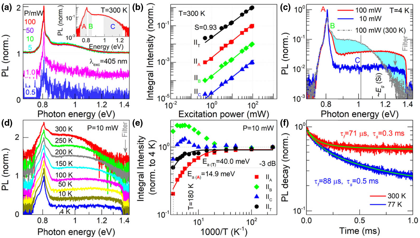
    Fig. 1. PL spectra. (a) Room-temperature PL spectra from the Er/O-doped Si at different excitation powers (P). PL curves are tentatively divided into three parts, marked by A, B and C, as shown in the inset. (b) Excitation power dependence of PL integral intensity (II) at 300 K. (c) PL spectra at P=10  mW (blue curve) and 100 mW (red curve) at 4 K. The room-temperature PL result at P=100  mW (gray curve) is also given for comparison. (d) PL spectra at different temperatures (P=10  mW). (e) Arrhenius plot of normalized PL integral intensity versus inversed temperature. (f) PL decay curves at 77 and 300 K together with the fitting results.
    EL spectra and analysis. (a) Schematic illustration of the LED structure. (b) Current-dependent EL spectra at 300 K. (c) PC spectrum at 300 K (upper panel). The star “*” marks the maximum of the third-order derivative and the blue line Eg(Si)=1.10 eV. The PC shoulder at ∼0.81 eV is from the Er-related defects. The lower panel shows the EL and PL spectra of the LED at 300 K. (d)–(g) Current dependence of the EL peak energy, FWHM, intensity, and integrated intensity, respectively, at 300 K (red) and 7 K (blue). The green lines are guides to the eyes.
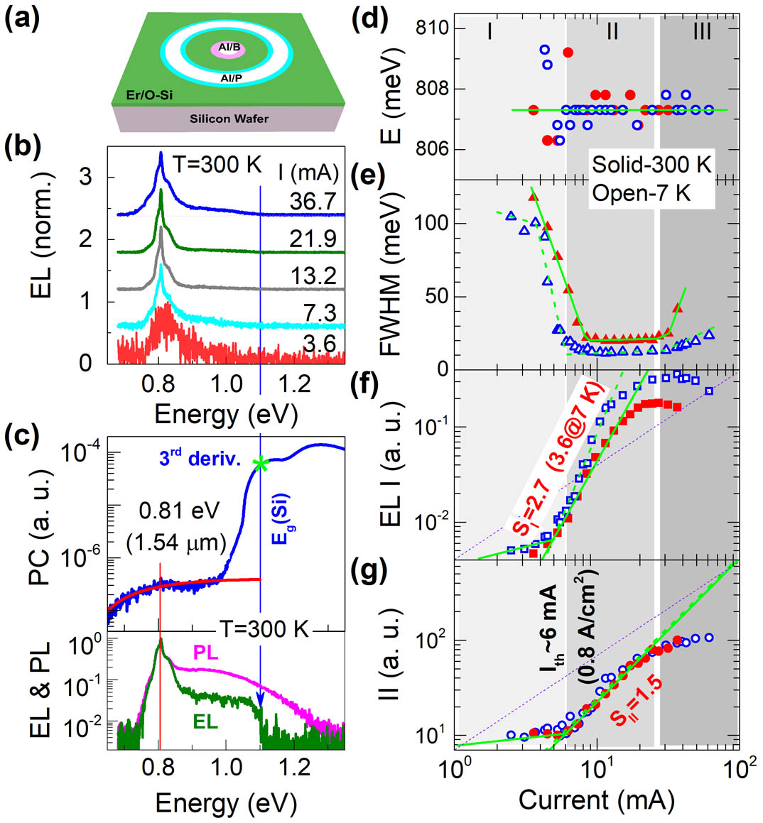
    Fig. 2. EL spectra and analysis. (a) Schematic illustration of the LED structure. (b) Current-dependent EL spectra at 300 K. (c) PC spectrum at 300 K (upper panel). The star “*” marks the maximum of the third-order derivative and the blue line Eg(Si)=1.10  eV. The PC shoulder at 0.81  eV is from the Er-related defects. The lower panel shows the EL and PL spectra of the LED at 300 K. (d)–(g) Current dependence of the EL peak energy, FWHM, intensity, and integrated intensity, respectively, at 300 K (red) and 7 K (blue). The green lines are guides to the eyes.
    Spatially resolved intensity distribution at the emitting surface of the LED at 1.54 μm (a) below and (b) above the threshold current. The emission imaging of the surface is also shown at the bottom for comparison. The imaging region of EL is the area between two electrodes.
    Fig. 3. Spatially resolved intensity distribution at the emitting surface of the LED at 1.54 μm (a) below and (b) above the threshold current. The emission imaging of the surface is also shown at the bottom for comparison. The imaging region of EL is the area between two electrodes.
    TR-PL spectral results. (a) TR-PL image from the Er/O-doped Si at 5 K (left) with a 760 nm excitation laser. (b) Time-integrated spectrum and Gaussian fit. (c) Decay curves of the sample and the laser. (d) Time-integrated spectra at excitation wavelengths of 760 and 380 nm. (e) Decay curves at different excitation wavelengths.
    Fig. 4. TR-PL spectral results. (a) TR-PL image from the Er/O-doped Si at 5 K (left) with a 760 nm excitation laser. (b) Time-integrated spectrum and Gaussian fit. (c) Decay curves of the sample and the laser. (d) Time-integrated spectra at excitation wavelengths of 760 and 380 nm. (e) Decay curves at different excitation wavelengths.
    Scheme of the carrier relaxation dynamics. The hot carriers in the upper states at Γ′ or L points excited by the 380 nm laser transfer to the indirect CB minimum (Δ1c) of Si with a time constant of ∼110 ps. From here, a time constant of ∼30 ps characterizes the transition of carriers to the distributed band created by the Er/O-related donor states.
    Fig. 5. Scheme of the carrier relaxation dynamics. The hot carriers in the upper states at Γ or L points excited by the 380 nm laser transfer to the indirect CB minimum (Δ1c) of Si with a time constant of 110  ps. From here, a time constant of 30  ps characterizes the transition of carriers to the distributed band created by the Er/O-related donor states.
    Schematic representation of the fabrication procedure to form (a) Er/O-doped Si samples and (b) LED devices.
    Fig. 6. Schematic representation of the fabrication procedure to form (a) Er/O-doped Si samples and (b) LED devices.
    Concentration and electrical characterization of Er/O-doped Si LEDs. (a) Erbium (green line) and oxygen (purple line) and (b) boron (red line) and phosphorous (blue line) ion distribution profiles on their respective implantation region of Er/O-doped Si devices by secondary ion mass spectroscopy (SIMS) measurement. (c) I−V curves of the diode devices.
    Fig. 7. Concentration and electrical characterization of Er/O-doped Si LEDs. (a) Erbium (green line) and oxygen (purple line) and (b) boron (red line) and phosphorous (blue line) ion distribution profiles on their respective implantation region of Er/O-doped Si devices by secondary ion mass spectroscopy (SIMS) measurement. (c) IV curves of the diode devices.
    Transmission and reflectance spectra of the Er-doped Si with or without application of the DC technique at 300 K. For comparison, the results of the pure Si after double-side polish or single-side polish are also shown. (a) The transmission spectra of the polished-pure and Er-doped Si at 300 K; (b) the corresponding absorption coefficient spectra from (a); (c) the transmission spectra of the Er-doped Si obtained by the DC technique at different temperatures; (d) the reflectance spectra.
    Fig. 8. Transmission and reflectance spectra of the Er-doped Si with or without application of the DC technique at 300 K. For comparison, the results of the pure Si after double-side polish or single-side polish are also shown. (a) The transmission spectra of the polished-pure and Er-doped Si at 300 K; (b) the corresponding absorption coefficient spectra from (a); (c) the transmission spectra of the Er-doped Si obtained by the DC technique at different temperatures; (d) the reflectance spectra.
    Comparison of normalized PL spectra of Er-doped Si samples by RTA and DC processes in a semi-logarithmic plot (a) at 5 K and (b) at 300 K.
    Fig. 9. Comparison of normalized PL spectra of Er-doped Si samples by RTA and DC processes in a semi-logarithmic plot (a) at 5 K and (b) at 300 K.
    Jin Hong, Huimin Wen, Jiajing He, Jingquan Liu, Yaping Dan, Jens W. Tomm, Fangyu Yue, Junhao Chu, Chungang Duan. Stimulated emission at 1.54 μm from erbium/oxygen-doped silicon-based light-emitting diodes[J]. Photonics Research, 2021, 9(5): 714
    Download Citation