
Jin Hong, Huimin Wen, Jiajing He, Jingquan Liu, Yaping Dan, Jens W. Tomm, Fangyu Yue, Junhao Chu, Chungang Duan. Stimulated emission at 1.54 μm from erbium/oxygen-doped silicon-based light-emitting diodes[J]. Photonics Research, 2021, 9(5): 714
- Photonics Research
- Vol. 9, Issue 5, 714 (2021)
Abstract
1. INTRODUCTION
Silicon/Si-based light sources, including lasers at telecommunication wavelengths, are the bottleneck for the heterogeneous integration of photonics with complementary metal-oxide-semiconductor circuits [1–6]. Ion implantation of erbium (Er) (often with oxygen) into Si is believed to be one of the most promising approaches to create Si-based light-emitting devices (LEDs) at 1.54 μm [7–15]. However, the reported quantum efficiencies are extremely low () at room temperature, mainly due to strong nonradiative recombination caused by the comparably large Er-related precipitates formed during the cooling process in the standard rapid thermal annealing (RTA) [3,15–17]. Recently, the efficiency has been substantially improved by introducing a deep cooling (DC) technique [11] that can effectively mitigate the Er precipitation created during the RTA process. LEDs with a perpendicular emission structure based on the obtained material achieved a record external quantum efficiency of at room temperature [11].
Here, by optimizing the implantation of Er and O, the DC procedure, and the Si-based LED structure with a planar emission geometry, a near-unity quantum yield (or slope efficiency) of the photoluminescence (PL) in Er-doped Si is reached. Moreover, a superlinearly growing electroluminescence (EL) is obtained with a slope efficiency beyond 2 even at room temperature. The low threshold of () [18,19], the superlinear EL integral intensity [20–22], the narrowing full width at half-maximum (FWHM) [23,24], and the Gaussian-like spatial emission distribution [25–29] confirm the presence of stimulated emission involving transitions related to the [30–33]. Time-resolved PL (TR-PL) and photocurrent (PC) measurements reveal the relaxation dynamics of the nonequilibrium carriers from the Si host to the precipitates. The hot nonequilibrium carriers in Si first cross the intravalley barrier (e.g., or L point in -space if the laser energy is high enough) with a time constant of to the bottom of the indirect conduction band (CB) (or the point) [34,35]. The excess carriers further decay from the CB bottom to the evenly distributed Er/O-related complexes that act as a quasi-continuous donor band with a decay time of . Within this donor band, the carriers resonantly excite (i.e., transfer the energy of carriers by nonradiative recombination to) the -4f electrons to emit at ().
2. MATERIALS AND METHODS
A. Sample Fabrication
Float zone intrinsic Si (100) wafers (resistivity: ; thickness: ; Suzhou Resemi Semiconductor Co., Ltd, China) were used. Er and O ions were implanted with an injection energy and dose of 200 keV and , and 32 keV and , respectively, at the Institute of Semiconductors, Chinese Academy of Sciences, China. After that, the Er/O-implanted Si samples were cleaned with ethanol and deionized water, and then they were immersed in a piranha solution (sulfuric acid:30% hydrogen ) for 30 min at 90°C, followed by drying with a high-purity nitrogen (99.99%) stream. To form a planar p–n junction, we further implanted boron (B) and phosphorus (P) dopants into these Si samples (B: 30 keV and ; P: 80 keV and ). They have a similar peak concentration located below the surface, which matches the peak depth of the Er in Si. Then 200 nm thick films were deposited on the Er/O-implanted Si samples by reactive magnetron sputtering (Delton multitarget magnetic control sputtering system, AEMD, SJTU). A DC process was performed to activate the Er/O, B, and P dopants at the same time via an upgraded dilatometer (DIL 805A, TA Instruments) [11], where the samples were annealed at 950°C for 5 min by means of copper-coil-based electromagnetic heating and followed by a flush of high-purity He (99.999%) gas cooled in liquid (77 K). Detailed descriptions can be found in our previous work in Ref. [11].
Sign up for Photonics Research TOC. Get the latest issue of Photonics Research delivered right to you!Sign up now
A pair of coaxial electrodes was prepared by UV photolithography (MDA-400M, MIDAS) and metal film deposition (Nexdep, Angstrom Engineering Inc.). The internal electrode is in contact with the -type boron doping region, and the external electrode in contact with the -type P region. The schematic representations of the fabrication procedure to form Er/O-doped Si samples and LEDs are shown in Fig. 6 in Appendix A. All the microfabrication processes were performed with home-built devices at the Center for Advanced Electronic Materials and Devices, Shanghai Jiao Tong University. After the Al metal wire bonding (7476D, West Bond), the devices were integrated on a printed circuit board. The curves were taken using a digital sourcemeter (Keithley 2400) controlled by a LabVIEW script.
B. Optical Characterizations
A Fourier transform infrared (FTIR) spectrometer (Vertex 80v, Bruker) was employed to measure transmission, reflectance, steady-state PL and EL, and PC spectra. The focused 405 nm emission from a continuous-wave (cw) laser diode (MLL-III-405, CNI, Changchun, China) with a maximum excitation power of was employed as the excitation source. The effective excitation power on the sample surface was calibrated by referring to the 405 nm transmission and reflectance of the samples at different temperatures. Different optical filters including notch filters, neutral density filters, and long-pass filters were utilized for avoiding the influence of the excitation during the excitation-power-dependent PL measurements. For EL measurements, cw and pulsed [with a nanosecond (ns) to microsecond (μs) pulse duration and a repetition rate of ] currents were injected into the structures. For PC measurements, a low-noise current preamplifier (SRS SR570) was employed for recording the defect-related PC signal below the band gap of Si.
TR-PL was carried out in order to determine the nonequilibrium carrier lifetime related to . This was implemented by milliwatt (mW) excitation with a 405 nm emitting diode laser being operated at 3 kHz as the excitation source, a fast InGaAs photodiode, and a gigahertz (GHz) sampling oscilloscope (Agilent MSO9404A) for data accumulation and readout. Simultaneously, the PL decay curve was cross-checked by a luminescence spectrometer. TR-PL at an 80 MHz repetition rate was implemented by using a Tsunami Ti:sapphire laser (760 or 380 nm by using second harmonic, spot size ) with 80 fs excitation pulses. The maximum energy density per pulse amounts to 57 and at 780 and 390 nm, respectively. Detection was made by a Hamamatsu C5680 streak camera with S1 photocathode operated in synchro-scan mode. The overall temporal resolution of the setup (1/e decay of an 80 fs pulse) is better than 10 ps. In all setups the samples were mounted on the cold head of a helium closed-cycle cooler. This allows for temperature adjustment from 4 K to ambient.
Near infrared EL imaging from the Er/O-Si LEDs was obtained at room temperature under an optical microscope (BX53M, Olympus) equipped with a near-infrared camera (C12471-03, Hamamatsu). The recorded video is provided in Appendix B (see
3. RESULTS AND DISCUSSION
A. Precharacterization by PL Measurements
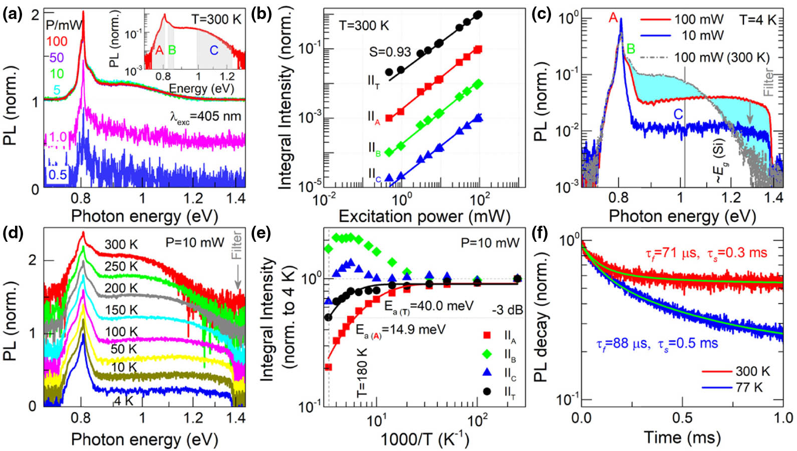
Figure 1.PL spectra. (a) Room-temperature PL spectra from the Er/O-doped Si at different excitation powers (
To have a deeper insight into the above process, the integral intensities of the main peak A, the side shoulder B, and the tail C are normalized to their integral intensity at 4 K. The normalized integral intensities are shown in the Arrhenius plot in Fig. 1(e). While the main peak A quenches monotonously with increase of temperature, emissions of B and C first increase and then decrease at a critical temperature point of (). Moreover, the total integral PL intensity also shows a monotonous decrease but with a relatively low temperature-quenching rate at 300 K (still of 4 K, i.e., with a decrease of 3 dB). This means that excitons transfer between the states, which are involved in the generation of the emission bands A, B, and C, without being affected by strong temperature-dependent nonradiative recombination. Based on the evolutions in Fig. 1(e), an activation energy of can be extracted for the main peak A (rather close to the phonon energy of ) [15] and one of for the total emission. Figure 1(f) shows the PL decay of the 1.54 μm emission at 300 K and 77 K for an excitation power of . The transient PL decays following a biexponential function with a slow (, ) and a fast (, ) component. The slow one is the lifetime of spontaneous emission, slightly shorter than the ∼millisecond (ms) lifetime of the in Refs. [11,36]. The fast one could be attributed to the carrier relaxation between the sublevels of , which will be further discussed later.
B. Electrically Pumped Stimulated Emission
![]()
Figure 2.EL spectra and analysis. (a) Schematic illustration of the LED structure. (b) Current-dependent EL spectra at 300 K. (c) PC spectrum at 300 K (upper panel). The star “*” marks the maximum of the third-order derivative and the blue line
To further clarify the energetic structure in the LEDs, we recorded the short-circuit PC spectra at 300 K under light illumination from 0.6 to 1.3 eV in photon energy as shown in Fig. 2(c). The third-order derivative of the curve sets the cutoff at , which corresponds to the Si band gap . It is necessary to point out that around 0.1 eV below the Si band gap, the PC reaches a plateau after an exponential decline by 2 orders of magnitude, which extends to before it drops below the background noise. This PC plateau roughly lies in the same spectral range of the broad EL band, and it should come from the Er-related defect (including -4f degenerated) states [37]. Taking into account the PC and EL bands from 0.7 to 1.1 eV, this implies that a quasi-continuous band from 0.7 eV above the valence band (VB) to the bottom of (or even above) the CB is formed.
Figures 2(d) and 2(e) show the main peak positions and FWHMs as functions of the injection current at 300 and 7 K. It can be observed that the main emission peak at 1.54 μm is almost independent of the injection current, whereas the FWHM gives a visible reduction until the current approaches . After a saturation region, the FWHM starts to broaden again when the injection current is higher than . Moreover, in Figs. 2(f) and 2(g), as the injection current ramps up, the peak intensity and integral intensity distinctively show a sublinear increase followed by superlinear ramp with a slope of at 300 K ( at 7 K) and at 300 K (almost the same at 7 K), respectively. A well-pronounced threshold is observed at or [refer to the integral intensity in Fig. 2(g)]. These features, along with the visible reduction of FWHM, suggest that amplified spontaneous [20,22,23] (or stimulated [32,33]) emission occurs in our Si LEDs. Clearly, the LED device operates in three different modes and transits sequentially from Mode I to II and to III as the current increases [see Figs. 2(d)–2(g)], in which Mode I represents the transition from spontaneous to amplified spontaneous emission; Mode II is the typical stimulated radiation with a distinctive superlinearity of the peak and integral intensity; and Mode III is the one in which the radiation recombination starts to be suppressed by the thermal effect of high injection current ().
The emission cross section can be thus estimated by the following equation [29,38]:
![]()
Figure 3.Spatially resolved intensity distribution at the emitting surface of the LED at 1.54 μm (a) below and (b) above the threshold current. The emission imaging of the surface is also shown at the bottom for comparison. The imaging region of EL is the area between two electrodes.
C. Carrier Relaxation Dynamics by Time-Resolved PL
![]()
Figure 4.TR-PL spectral results. (a) TR-PL image from the Er/O-doped Si at 5 K (left) with a 760 nm excitation laser. (b) Time-integrated spectrum and Gaussian fit. (c) Decay curves of the sample and the laser. (d) Time-integrated spectra at excitation wavelengths of 760 and 380 nm. (e) Decay curves at different excitation wavelengths.
When the frequency-doubled wavelength (380 nm) excites the sample, a similar but smaller emission band at was observed; see Fig. 4(d). In the time domain, the emission has two striking features shown in Fig. 4(e). First, unlike the long emission lifetime excited at the wavelength of 760 nm, the emission has a short decay time of . Second, the emission lags behind the excitation pulse by . These features are likely caused by the fact that high-energy photons from the 380 nm laser can excite electrons from the VB to the L (or ) point of the CB, which the 760 nm laser excitation cannot do. With assistance of phonons, hot electrons from the L point will first transit to the CB bottom ( point) and then emit photons at via radiative recombination from band to band. It should be emphasized that the time difference of cannot be the coupling-related error of the test system, since the drift of the system, i.e., the desynchronization, is about 5 ps per hour in the synchro-scan regime. It could be then attributed to the transfer time of the carriers across the intravalley barrier. The relatively long transit time results in a low concentration of excess carriers at the CB bottom because the barrier temporally holds the carriers at the L point. As a result, excess carriers do not generate strong spontaneous emission but rapidly () relax to the Er/O-related quasi-continuous levels below the indirect CB of Si [15,16]; see more discussion later. This behavior is illustrated by the blue transients in Fig. 4(e). This fast relaxation process suggests a fundamental discrepancy with the existing model of energy transfer from electron–hole pair recombination directly to the excitation of the -4f electrons for the 1.54 μm emission [40].
![]()
Figure 5.Scheme of the carrier relaxation dynamics. The hot carriers in the upper states at
Notice that the sublevels of excited and ground states have an energy separation of about 10–15 meV between the first-lying and second-lying crystal field split levels of the first () excited state [40]. Since the activation energy for band A (1.54 μm) is 14.9 meV and the electrons in band A are thermally excited to band B as shown in Fig. 1(e), the emission center of bands A and B is likely related to the first-lying and the second-lying split levels of and to the sublevels of () the ground state, respectively. As for the activation energy of for the entire emission signal in this material system, it can be tentatively ascribed to the co-contributions of the reversed transfer of the nonequilibrium carriers from the impurity-related band C to the Si and the potential nonradiative recombination of carriers of band C via electron-phonon coupling.
What needs to be emphasized again is that the results achieved are largely due to the use of the DC process in sample preparation. The process offers advantages for the optically pumped . These ions appear in high density in relatively uniformly sized, Er-related clusters with a diameter of , which is much smaller than the 5 nm diameter achieved with the standard RTA process [11]. Moreover, the spatial distribution of the small clusters is extremely even, which provides very useful conditions for the Er/O cluster to act as a broad and quasi-continuous donor band [42]. The decaying carriers from the Si host into the Er-related states excite the 4f electron of , which produces the emission at . Details on material characterizations by high-resolution transmission electron microscopy and X-ray photoelectron spectroscopy have been described in Ref. [11], and the striking difference of the defect-related PL signal between RTA and DC is shown in Fig. 9 in Appendix C.
4. CONCLUSIONS
In conclusion, we observed amplified spontaneous (or stimulated) emissions at room temperature with a low threshold of from Er/O-doped Si-based LEDs that were treated with a DC process. In comparison with the standard RTA process, the DC process can effectively suppress the precipitation of Er/O-related nanocrystals and form more uniformly distributed Er-O-Si compounds. The impact of the DC process on Er/O formation can effectively reduce the density of nonradiative defects in the Si band gap and facilitate the formation of a quasi-continuous Er/O-related donor band right below the Si CB. As a result, strong room-temperature PL and amplified spontaneous (or stimulated) emissions were directly observed for them. In particular, the quasi-continuous Er/O-related donor band not only facilitates the rapid emission decay of excess carriers but also serves as efficient recombination centers to extend the emissions up to the Si band gap, forming a broad tail in the spectrum in addition to the widely observed emission at 1.54 μm. This work may pave the way for fabricating superluminescent (or laser) diodes at communication wavelengths based on rare-earth-doped silicon.
Acknowledgment
Acknowledgment. The authors thank Dr. Ren Zhu for the characterization of spatially resolved intensity distribution at the emitting surface of the LED.
APPENDIX A: SCHEMATIC OF THE FABRICATION PROCEDURE
![]()
Figure 6.Schematic representation of the fabrication procedure to form (a) Er/O-doped Si samples and (b) LED devices.
![]()
Figure 7.Concentration and electrical characterization of Er/O-doped Si LEDs. (a) Erbium (green line) and oxygen (purple line) and (b) boron (red line) and phosphorous (blue line) ion distribution profiles on their respective implantation region of Er/O-doped Si devices by secondary ion mass spectroscopy (SIMS) measurement. (c)
APPENDIX B: NEAR-INFRARED EL IMAGING FROM THE Er/O-Si LEDs
This video (
APPENDIX C: COMPARISON OF TRANSMISSION, REFLECTANCE, AND NORMALIZED PL SPECTRA OF Er-DOPED Si SAMPLES BY RTA AND DC PROCESSES
Figures?
![]()
Figure 8.Transmission and reflectance spectra of the Er-doped Si with or without application of the DC technique at 300 K. For comparison, the results of the pure Si after double-side polish or single-side polish are also shown. (a) The transmission spectra of the polished-pure and Er-doped Si at 300 K; (b) the corresponding absorption coefficient spectra from (a); (c) the transmission spectra of the Er-doped Si obtained by the DC technique at different temperatures; (d) the reflectance spectra.
![]()
Figure 9.Comparison of normalized PL spectra of Er-doped Si samples by RTA and DC processes in a semi-logarithmic plot (a) at 5 K and (b) at 300 K.
References
[1] X. Chen, M. M. Milosevic, S. Stanković, S. Reynolds, T. D. Bucio, K. Li, D. J. Thomson, F. Gardes, G. T. Reed. The emergence of silicon photonics as a flexible technology platform. Proc. IEEE, 106, 2101-2116(2018).
[2] D. Thomson, A. Zilkie, J. E. Bowers, T. Komljenovic, G. T. Reed, L. Vivien, D. Marris-Morini, E. Cassan, L. Virot, J.-M. Fédéli. Roadmap on silicon photonics. J. Opt., 18, 073003(2016).
[3] Z. Zhou, B. Yin, J. Michel. On-chip light sources for silicon photonics. Light Sci. Appl., 4, e358(2015).
[4] H. Subbaraman, X. Xu, A. Hosseini, X. Zhang, Y. Zhang, D. Kwong, R. T. Chen. Recent advances in silicon-based passive and active optical interconnects. Opt. Express, 23, 2487-2511(2015).
[5] D. Liang, J. E. Bowers. Recent progress in lasers on silicon. Nat. Photonics, 4, 511-517(2010).
[6] D. A. Miller. Device requirements for optical interconnects to silicon chips. Proc. IEEE, 97, 1166-1185(2009).
[7] E. M. Fadaly, A. Dijkstra, J. R. Suckert, D. Ziss, M. A. van Tilburg, C. Mao, Y. Ren, V. T. van Lange, K. Korzun, S. Kölling. Direct-bandgap emission from hexagonal Ge and SiGe alloys. Nature, 580, 205-209(2020).
[8] C. Roques-Carmes, S. E. Kooi, Y. Yang, A. Massuda, P. D. Keathley, A. Zaidi, Y. Yang, J. D. Joannopoulos, K. K. Berggren, I. Kaminer. Towards integrated tunable all-silicon free-electron light sources. Nat. Commun., 10, 3176(2019).
[9] S. Chen, W. Li, J. Wu, Q. Jiang, M. Tang, S. Shutts, S. N. Elliott, A. Sobiesierski, A. J. Seeds, I. Ross. Electrically pumped continuous-wave III–V quantum dot lasers on silicon. Nat. Photonics, 10, 307-311(2016).
[10] Y. Takahashi, Y. Inui, M. Chihara, T. Asano, R. Terawaki, S. Noda. A micrometre-scale Raman silicon laser with a microwatt threshold. Nature, 498, 470-474(2013).
[11] H. Wen, J. He, J. Hong, S. Jin, Z. Xu, H. Zhu, J. Liu, G. Sha, F. Yue, Y. Dan. Efficient Er/O-doped silicon light-emitting diodes at communication wavelength by deep cooling. Adv. Opt. Mater., 8, 2000720(2020).
[12] M. A. Hughes, H. Li, N. Theodoropoulou, J. D. Carey. Optically modulated magnetic resonance of erbium implanted silicon. Sci. Rep., 9, 1(2019).
[13] M. Celebrano, L. Ghirardini, M. Finazzi, G. Ferrari, Y. Chiba, A. Abdelghafar, M. Yano, T. Shinada, T. Tanii, E. Prati. Room temperature resonant photocurrent in an erbium low-doped silicon transistor at telecom wavelength. Nanomaterials, 9, 416(2019).
[14] M. Lourenço, M. Milošević, A. Gorin, R. Gwilliam, K. Homewood. Super-enhancement of 1.54 μm emission from erbium co-doped with oxygen in silicon-on-insulator. Sci. Rep., 6, 1(2016).
[15] A. Kenyon. Erbium in silicon. Semicond. Sci. Tech., 20, R65-R84(2005).
[16] N. Q. Vinh, N. N. Ha, T. Gregorkiewicz. Photonic properties of Er-doped crystalline silicon. Proc. IEEE, 97, 1269-1283(2009).
[17] G. Franzò, F. Priolo, S. Coffa. Understanding and control of the erbium non-radiative de-excitation processes in silicon. J. Lumin., 80, 19-28(1998).
[18] H. Shen, D.-S. Li, D.-R. Yang. Research progress of silicon light source. Acta Phys. Sin., 64, 204208(2015).
[19] S. Wu, S. Buckley, J. R. Schaibley, L. Feng, J. Yan, D. G. Mandrus, F. Hatami, W. Yao, J. Vučković, A. Majumdar. Monolayer semiconductor nanocavity lasers with ultralow thresholds. Nature, 520, 69-72(2015).
[20] J. Hong, H. Wang, F. Yue, J. W. Tomm, D. Kruschke, C. Jing, S. Chen, Y. Chen, W. Hu, J. Chu. Emission kinetics from PbSe quantum dots in glass matrix at high excitation levels. Phys. Status Solidi R, 12, 1870312(2018).
[21] J. Ramírez, F. F. Lupi, Y. Berencén, A. Anopchenko, J. Colonna, O. Jambois, J. Fedeli, L. Pavesi, N. Prtljaga, P. Rivallin. Er-doped light emitting slot waveguides monolithically integrated in a silicon photonic chip. Nanotechnology, 24, 115202(2013).
[22] T. Kobayashi, M. Djiango, W. J. Blau. Near-infrared electroluminescence and stimulated emission from semiconducting nonconjugated polymer thin films. J. Appl. Phys., 107, 023103(2010).
[23] V. Ho, Y. Wang, B. Ryan, L. Patrick, H. Jiang, J. Lin, N. Vinh. Observation of optical gain in Er-doped GaN epilayers. J. Lumin., 221, 117090(2020).
[24] N. T. Otterstrom, R. O. Behunin, E. A. Kittlaus, Z. Wang, P. T. Rakich. A silicon Brillouin laser. Science, 360, 1113-1116(2018).
[25] H. Liu, Z. Li, W. Song, Y. Yu, F. Pang, T. Wang. MoS2/graphene heterostructure incorporated passively mode-locked fiber laser: from anomalous to normal average dispersion. Opt. Mater. Express, 10, 46-56(2020).
[26] S. Saito, T. Takahama, K. Tani, M. Takahashi, T. Mine, Y. Suwa, D. Hisamoto. Stimulated emission of near-infrared radiation in silicon fin light-emitting diode. Appl. Phys. Lett., 98, 261104(2011).
[27] V. Robbiano, G. M. Paternó, A. A. La Mattina, S. G. Motti, G. Lanzani, F. Scotognella, G. Barillaro. Room-temperature low-threshold lasing from monolithically integrated nanostructured porous silicon hybrid microcavities. ACS Nano, 12, 4536-4544(2018).
[28] K. Luterová, D. Navarro, M. Cazzanelli, T. Ostatnický, J. Valenta, S. Cheylan, I. Pelant, L. Pavesi. Stimulated emission in the active planar optical waveguide made of silicon nanocrystals. Phys. Status Solidi C, 2, 3429-3434(2005).
[29] A. Rapaport, M. Bass. The role of stimulated emission in luminescence decay. J. Lumin., 97, 180-189(2002).
[30] M. Bresler, O. Gusev, E. Terukov, I. Yassievich, B. Zakharchenya, V. Emel’yanov, B. Kamenev, P. Kashkarov, E. Konstantinova, V. Y. Timoshenko. Stimulated emission in erbium-doped silicon structures under optical pumping. Mater. Sci. Eng. B, 81, 52-55(2001).
[31] L. A. Coldren, S. W. Corzine, M. L. Mashanovitch. Diode Lasers and Photonic Integrated Circuits, 218(2012).
[32] V. Ho, T. A. Tahtamouni, H. Jiang, J. Lin, J. Zavada, N. Vinh. Room-temperature lasing action in GaN quantum wells in the infrared 1.5 μm region. ACS Photon., 5, 1303-1309(2018).
[33] M. Huda, S. Ali. A study on stimulated emission from erbium in silicon. Mater. Sci. Eng. B, 105, 146-149(2003).
[34] M. Schultze, K. Ramasesha, C. Pemmaraju, S. Sato, D. Whitmore, A. Gandman, J. S. Prell, L. Borja, D. Prendergast, K. Yabana. Attosecond band-gap dynamics in silicon. Science, 346, 1348-1352(2014).
[35] J. Noffsinger, E. Kioupakis, C. G. Van de Walle, S. G. Louie, M. L. Cohen. Phonon-assisted optical absorption in silicon from first principles. Phys. Rev. Lett., 108, 167402(2012).
[36] X. Wang, B. Wang, L. Wang, R. Guo, H. Isshiki, T. Kimura, Z. Zhou. Extraordinary infrared photoluminescence efficiency of Er0.1Yb1.9SiO5 films on SiO2/Si substrates. Appl. Phys. Lett., 98, 071903(2011).
[37] B. De Geyter, A. J. Houtepen, S. Carrillo, P. Geiregat, Y. Gao, S. t. Cate, J. M. Schins, D. Van Thourhout, C. Delerue, L. D. Siebbeles. Broadband and picosecond intraband absorption in lead-based colloidal quantum dots. ACS Nano, 6, 6067-6074(2012).
[38] W. J. Miniscalco, R. S. Quimby. General procedure for the analysis of Er3+ cross sections. Opt. Lett., 16, 258-260(1991).
[39] W. L. Ng, M. Lourenco, R. Gwilliam, S. Ledain, G. Shao, K. Homewood. An efficient room-temperature silicon-based light-emitting diode. Nature, 410, 192-194(2001).
[40] V. X. Ho, T. V. Dao, H. X. Jiang, J. Y. Lin, J. M. Zavada, S. A. McGill, N. Q. Vinh. Photoluminescence quantum efficiency of Er optical centers in GaN epilayers. Sci. Rep., 7, 1(2017).
[41] I. Costa, D. Pera, J. A. Silva. Improving light capture on crystalline silicon wafers. Mater. Lett., 272, 127825(2020).
[42] M. Bürkle, M. Lozac’h, C. McDonald, M. Macias-Montero, B. Alessi, D. Mariotti, V. Švrček. Tuning the bandgap character of quantum-confined Si-Sn alloyed nanocrystals. Adv. Funct. Mater., 30, 1907210(2020).

Set citation alerts for the article
Please enter your email address
© Copyright 2018-2021 | Chinese Laser Press. All Rights Reserved 沪ICP备15018463号-20