
Qixiang Cheng, Liang Yuan Dai, Nathan C. Abrams, Yu-Han Hung, Padraic E. Morrissey, Madeleine Glick, Peter O’Brien, Keren Bergman, "Ultralow-crosstalk, strictly non-blocking microring-based optical switch," Photonics Res. 7, 155 (2019)
- Photonics Research
- Vol. 7, Issue 2, 155 (2019)
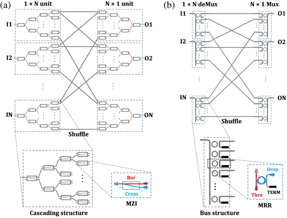
Fig. 1. (a) Switch-and-select topology with MZI elements arranged in a cascading structure. (b) Modified switch-and-select topology with MRR-based spatial (de)multiplexers.
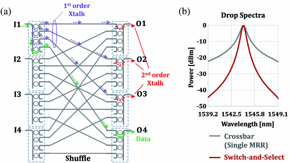
Fig. 2. (a) Schematic of a 4 × 4
Fig. 3. (a) Schematic layout of the 4 × 4 4 × 1
Fig. 4. (a) Schematic of a silicon die flip-chip bonded onto a PCB breakout board using solder bumps. A fiber array is attached to the edge of the silicon chip. (b) Photo of the packaged AIM chip.
Fig. 5. (a) Schematic of the device test bed. (b) Schematic of the control scheme of the switch-and-select switching circuit for the on and off states.
Fig. 6. Measured optical power map of the 4 × 4
Fig. 7. Schematic of test structures for (a) the Si/SiN two-layered intersections, and (b) Si/SiN interlayer couplers. (c) Simulated insertion loss and crosstalk as functions of interlayer separation for the two-layer intersections using Lumerical FDTD software. The left and right charts show the results for the Si and SiN waveguides, respectively.
Fig. 8. Crosstalk breakdown measurement. (a) Outlined optical paths under test: data routed in path 2-2 and the crosstalk leakage to output 1 (crosstalk 2-1). Measured power spectrum for (b) the data at output 2 and (c) crosstalk leakage at output 1 with thermal tuning on the second-stage output MRR to minimize the crosstalk leakage.
Fig. 9. (a) Power tuning for path 4-4 showing the path extinction ratio and the breakdown in on-off extinction from the first- and second-stage MRRs. (b) Crosstalk leakage to output 1, 2, and 3 for path 4-4. (c) Power tuning for path 2-3 and (d) crosstalk leakage for path 2-3.
Fig. 10. Normalized spectra of a set of representative paths. Resolution is set at 0.1 nm.
Fig. 11. BER as a function of received optical power at 12.5 Gb/s (a) for path 4-4 and B2B and for (b) path 2-3 and B2B. Insets show eye diagrams after the switch; (c) and (d) show the amplified eye diagrams for B2B and path 4-4 at 0 dBm.
Fig. 12. Measured optical time-domain response of the thermo-optic switch. The cursors show the 10%–90% power points for (a) the rise edge and (b) the fall edge.
|
Table 1. Component-Level Loss Estimation


Set citation alerts for the article
Please enter your email address

© Copyright 2018-2021 | Chinese Laser Press. All Rights Reserved 沪ICP备15018463号-20