Abstract
We report on the first monolithically integrated microring-based optical switch in the switch-and-select architecture. The switch fabric delivers strictly non-blocking connectivity while completely canceling the first-order crosstalk. The switching circuit consists of eight silicon microring-based spatial (de-)multiplexers interconnected by a Si/SiN dual-layer crossing-free central shuffle. Analysis of the on-state and off-state power transfer functions reveals the extinction ratios of individual ring resonators exceeding 25 dB, leading to switch crosstalk suppression of up to over 50 dB in the switch-and-select topology. Optical paths are assessed, showing losses as low as 0.1 dB per off-resonance ring and 0.5 dB per on-resonance ring. Photonic switching is actuated with integrated micro-heaters to give an passband. The fully packaged device is flip-chip bonded onto a printed circuit board breakout board with a UV-curved fiber array.1. INTRODUCTION
Modern data centers increasingly rely on optical interconnects for delivering critical communication connectivity among numerous servers. The photonic switch is a potential key element to meet the growing interconnection performance requirements in data center architectures [1]. Several technologies can enable spatial or wavelength-selective optical switching, including micro-electro mechanical systems (MEMSs) [2,3], liquid crystals on silicon (LCOSs) [4], beam-steering [5], semiconductor optical amplifiers (SOAs) [6,7], Mach–Zehnder interferometers (MZIs) [8–11], micro-ring resonators (MRRs) [12,13], and wavelength routing with tunable lasers [14]. Optical switching engines leveraging free-space optics have been commercialized, i.e., 3D MEMS, LCOS, and beam-steering; however, the rigorous calibration and installation of discrete components introduce considerable complexity that is ultimately reflected in the cost per port. To ensure low cost per port and eventual data center adoption, optical switching technologies must demonstrate a path towards high volume manufacturing. This is most likely to be implemented through lithography-based fabrication and high-level integration [1].
Integrated photonic switch fabrics have been extensively explored in indium phosphide [7,15] and silicon [3,9–13,16] platforms. Benefiting from the CMOS industry’s developed fabrication and manufacturing infrastructures, silicon photonic devices have quickly matured to monolithic integration of tens of thousands of components [3,9,10]. The large index contrast between the core (silicon) and cladding (silica) layers enables strong confinement of the lightwave and thus leads to a much smaller device footprint. Silicon exhibits a strong thermo-optic (T-O) coefficient (), which can be leveraged to tune the phase in tens of microseconds [17]. To benefit from nanosecond-scale switching time, the free-carrier dispersion effect offers the best all-silicon solution for electro-optic (E-O) switch fabrics.
The first demonstration of a micrometer (μm)-scale silicon ring resonator by Xu et al. stimulated the research of MRR-based photonic integrated circuits [18]. Because of their small footprint and low power consumption, silicon MRRs have been extensively studied as modulators, filters, and (de-)multiplexers. To date, MRR-based optical switches have been primarily implemented in crossbar-based topologies such as the optical crossbar switch [12] and the two-stage cascaded crossbar switch [13]. The wavelength-selective nature of an MRR unit requires wavelength alignment across the switching circuit, and various schemes for fast and efficient wavelength locking have been demonstrated [19–21]. The crossbar-type topology fits the add-drop nature of the MRR unit, but the switch performance is limited by the large path-dependent loss and the first-order crosstalk.
Sign up for Photonics Research TOC. Get the latest issue of Photonics Research delivered right to you!Sign up now
In this paper, we present the design and thorough characterization of the first, to our knowledge, monolithic microring-based optical switch implemented in the switch-and-select topology. This design offers strictly non-blocking connectivity and fully blocks the first-order crosstalk. A Si/SiN two-layered structure with escalating couplers is leveraged to eliminate waveguide crossings in the central shuffle network. Preliminary test results can be found in Ref. [22]. Here, we present a detailed analysis of the device performance from the component level to the circuit level, showing a full power map across all electrically connected paths and revealing ultralow-crosstalk impairment. The on-off extinction for individual ring resonators is examined. The passbands of optical connections are measured, and the bit error rate (BER) performance of 12.5 Gb/s data routing across the switch is verified. Discussion on the switch scalability is also provided. This demonstration shows a clear pathway towards high-performance optical switching circuits for data center applications.
2. DESIGN, FABRICATION, AND PACKAGING
A. Topology
The switch-and-select topology was first implemented using MZI switching elements [11]. It comprises two linear switching arrays connected by a passive central shuffle network, as shown in Fig. 1(a). Each switching unit is arranged in a cascading structure of stages with MZI cells, resulting in the total number of switching stages being . In this topology, each pair of input and output switching arrays is dedicated to a specific input to an output path, offering strictly non-blocking connectivity.
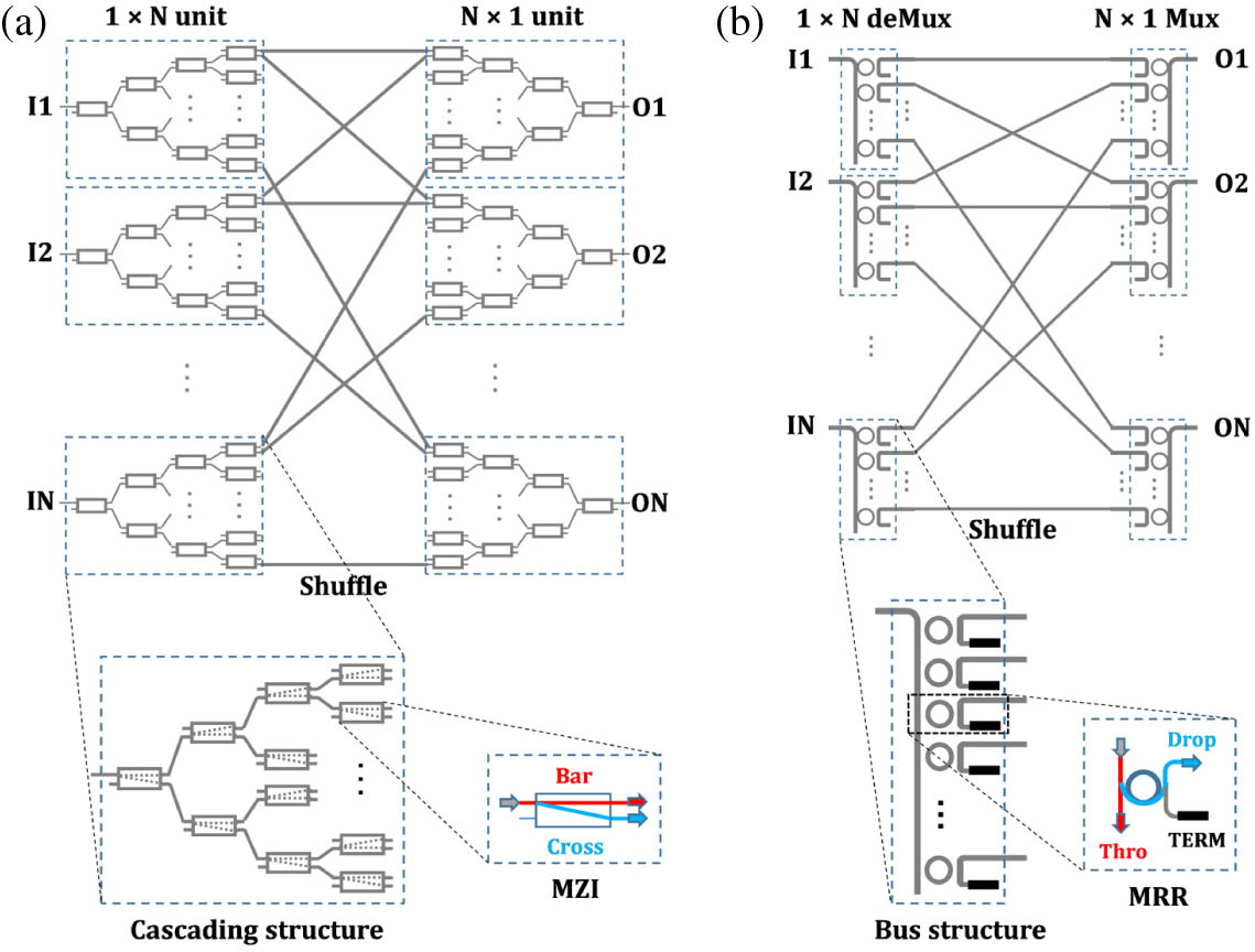
Figure 1.(a) Switch-and-select topology with MZI elements arranged in a cascading structure. (b) Modified switch-and-select topology with MRR-based spatial (de)multiplexers.
The switch-and-select architecture, however, can be considerably simplified by using MRR add-drop filters assembled in a bus structure acting as spatial (de)multiplexers, as shown in Fig. 1(b). Scale-up of such a design only requires adding microrings to the bus waveguides, which effectively reduces the scaling overhead in loss compared to that of the cascading scheme. The proposed design also maintains the number of drop (i.e., resonating) microrings in any path at two. An switch-and-select switching circuit has, in total, MRR elements. The central passive shuffle connects the th ring (element ) in the th input unit to the th ring (element ) in the th output unit. This brings a further advantage of self-routing as the optical connection of input to output occurs only when both element and rings are on resonance. The rest of the MRRs on the input and output units are adequately detuned from the resonance to ensure the maximum crosstalk suppression.
The MRR-based switch-and-select topology fully blocks the first-order crosstalk. For instance, in the device illustrated in Fig. 2(a), the optical path connects input 1 to output 4 (highlighted by green arrows) and the first-order crosstalk leakage to the off-resonance rings (outlined by purple arrows at the first, second, and third microrings) will get suppressed by another detuned microring at the output stage (marked by red arrows) before adding to the signal and hence experience two degrees of attenuation. This lowers the switch crosstalk level to the square of a single MRR element. Figure 2(b) compares the simulated drop spectrum of a single MRR element, e.g., in a crossbar switching device, and the switch-and-select structure. The latter exhibits a much sharper spectral edge. In this design, the add-drop MRR element is better to operate close to its critical coupling to maximize the extinction of resonance and minimize the drop loss. A detailed design space exploration of a silicon MRR element can be found in Ref. [23].

Figure 2.(a) Schematic of a switch-and-select switching circuit. Green, dashed purple, and dotted red arrows outline paths for data, first-order crosstalk, and second-order crosstalk, respectively. The solid semi-circles on MRRs indicate on-resonance coupling, while dashed semi-circles represent off-resonance coupling. (b) Comparison of simulated drop spectra of a single MRR element in a crossbar switching device and the switch-and-select structure.
It has been recognized that the fundamental limitation to the scalability of the switch-and-select topology is the waveguide crossings in the central shuffle network [24], which interconnects waveguides from the two linear switching arrays. Therefore, in this work, we investigate the dual-layer shuffle network that eliminates waveguide crossings.
B. Device Design and Fabrication
The layout of the microring-based switch-and-select switching circuit is schematically shown in Fig. 3(a). It comprises 32 add-drop ring resonators with integrated micro-heaters for on-chip tuning. Terminations are placed at the through port to eliminate optical reflections. The central shuffle network is implemented in a Si/SiN dual-layer structure with interlayer couplers, enabling a SiN waveguide to pass over a Si waveguide at intersections. Key parameters for such a dual-layer device include the width of the SiN waveguide (1 μm used in this work) and the separation between the two layers, determining the mode interaction and thus the loss and interlayer crosstalk. The intersections of the Si and SiN waveguides should be maintained at 90° for optimized performance. In this design, a few compromises are made for the intersections due to the limited chip space. An edge coupler array is used to couple light in and out of the chip. Two pairs of looped-back couplers are introduced to facilitate the coupling process.
Figure 3.(a) Schematic layout of the MRR-based switch-and-select switching fabric with insets showing the interlayer couplers. (b) Microscope photo of the fabricated device with insets of the enlarged MRR-based spatial multiplexer, the Si/SiN intersections, and the interlayer coupler.
The device was taped out using standard PDK elements through the AIM Photonics multi-project wafer run. A microscope photo of the fabricated device is shown in Fig. 3(b). The add-drop ring filters are placed at a pitch of 100 μm, and the measured shift of resonance shows a thermal efficiency of 1 nm/mW [17]. The switch fabric has a compact footprint of with 32 control electrodes and 2 common grounds. The edge coupler array has a pitch of 127 μm.
C. Packaging
The fabricated chip was packaged by the Tyndall National Institute using a flip-chip bonding process, as shown schematically in Fig. 4(a). The bare chip, with bond pads of pitch 100 μm, was first gold studded, and then solder was deposited using a PacTech solder jetter. The solder used in the process was SAC305, which has a 220°C melting point and provides solder balls with nominal diameters of 50 μm. The photonic integrated circuit (PIC) was flip-chip bonded onto a custom designed printed circuit board (PCB) breakout board. The board and PIC were co-designed, so that after bonding the PIC overhangs the edge of the PCB by . This overhang allowed a lidless, 48 channel fiber array to be butt coupled to the PIC. The fiber array was optically aligned to the waveguides and attached using a UV curable epoxy. Ribbon cables were used to fan out the electrical connections. The packaged device was mounted onto an aluminum assembly and the completed package is shown in Fig. 4(b).
Figure 4.(a) Schematic of a silicon die flip-chip bonded onto a PCB breakout board using solder bumps. A fiber array is attached to the edge of the silicon chip. (b) Photo of the packaged AIM chip.
3. CHARACTERIZATION
A. Optical Power Map
The operation of the optical switching circuit is first characterized in terms of on-state and off-state power transfer functions for each path. This gives a full optical power map of the device showing the optical insertion loss and crosstalk ratio across different paths. Figure 5(a) shows the test bed. A tunable laser is used to launch a continuous-wave signal at the wavelength of 1542.3 nm, which is selected to be close to the half free spectral range (FSR) of MRRs to the resonance for maximum extinction. The control scheme is schematically shown by Fig. 5(b). This also ensures that the operating wavelength has the minimum interaction with the bypass ring resonators. The on state and off state for each path are identified by tuning the bias voltage to reach the highest and lowest output power, respectively. The output is connected to an optical spectrum analyzer (OSA) to record both the peak transfer power and the spectrum. Figure 6 shows the measured optical power map of the MRR-based switch-and-select device with the red rectangle outlining the crosstalk leakage. Data on 13 optical paths are recorded out of the total 16 paths due to three electrical open circuits. Measurement on the looped-back edge couplers indicates a coupling loss between the chip and fiber of 5.5 dB per facet.
Figure 5.(a) Schematic of the device test bed. (b) Schematic of the control scheme of the switch-and-select switching circuit for the on and off states.
Figure 6.Measured optical power map of the MRR-based switch-and-select device. The red rectangle outlines the crosstalk leakage.
B. Optical Loss Analysis
Optical paths exhibit on-chip losses in the range of 1.8–20.4 dB as presented in Fig. 6. The large path-dependent loss is attributed to the high excess loss of escalating to and from the SiN layer. The passive loss of each path is a linear combination of different components; however, a large variation was observed for the SiN elements. As mentioned in Section 2.B, the few intersections that have an angle of between the Si and SiN waveguides do indeed compromise the loss, but it is suspected that the SiN waveguide and bending structure bring about excess loss, which requires further investigation.
Referring back to Fig. 3(a), paths 1-1 and 4-4 are both defined only in the Si layer and have no interaction with the SiN layer, representing the optimal cases. They both incorporate three off-resonance MRRs and two on-resonance ones; therefore, the 0.5 dB difference in loss (1.8 dB for path 4-4 and 2.3 dB for path 1-1) comes from the signal propagation in different waveguide lengths, showing the Si waveguide propagating loss to be 2.5 dB/cm.
The Si/SiN intersection loss and the interlayer coupling loss are assessed by two additional test structures, shown by Figs. 7(a) and 7(b), respectively. The intersection loss is measured to be on the Si waveguide. This is believed to be primarily caused by the mode interaction with the overpassed SiN layer due to the limited separation distance. Study of the Si/SiN interlayer mode interaction for transmission loss and crosstalk as functions of the separation using Lumerical finite-difference time-domain (FDTD) software is shown in Fig. 7(c). Minimizing the dual-layer performance penalty requires separation. Future designs will leverage the triple-layer platform developed by AIM Photonics, in which a SiN transfer layer is inserted in between to ensure adequate separation between the Si and the second SiN layer. The interlayer couplers are characterized to have 4 dB loss per pair (2 dB per facet), which is quite off from the predicted results. This could well be caused by imperfect fabrication and can be improved in the future. Fitting the test results back to paths 1-2, 2-1, 4-3, and 4-4, which have various numbers of off-resonance rings, we can estimate the loss for the MRR drop and through states, which is 0.5 dB and 0.1 dB, respectively. The component-level loss estimation is summarized in Table 1.
| Item | Loss |
| Si waveguide propagation | 2.5 dB/cm |
| MRR drop | 0.5 dB |
| MRR through | 0.1 dB |
| Si/SiN intersection | 0.15 dB |
| Si/SiN interlayer coupler | 2 dB/facet |
| Edge coupler | 5.5 dB/facet |
Table 1. Component-Level Loss Estimation
Figure 7.Schematic of test structures for (a) the Si/SiN two-layered intersections, and (b) Si/SiN interlayer couplers. (c) Simulated insertion loss and crosstalk as functions of interlayer separation for the two-layer intersections using Lumerical FDTD software. The left and right charts show the results for the Si and SiN waveguides, respectively.
C. Extinction and Crosstalk
Off-state signals are required to be maximally extinguished. The sum of leakage from any off-state path contributes to a path-dependent crosstalk. The on-off extinction of the individual ring resonators is thus a key parameter.
Figure 8 presents the crosstalk breakdown measurements to reveal the on-off extinction of individual ring elements that contribute to the crosstalk suppression. As illustrated by Fig. 8(a), data is routed through path 2-2, and the crosstalk leakage is monitored at output 1. In the outlined input spatial deMux unit, the first MRR (element ) is at an off-resonance state to let the data bypass, while the second ring element (element ) is on resonance to drop the signal. The data is then routed to output 2 by tuning the corresponded MRR at the second output Mux unit. The measured spectrum is shown by Fig. 8(b). The second MRR at the first output Mux unit (element ), which receives the crosstalk leakage, is first set at the on-resonance state. The spectrum is presented by the light blue line in Fig. 8(c), and compared to that of the Fig. 8(b), the difference shows the first-order crosstalk suppression between the ring and ring (25.1 dB). The subsequent tuning of the ring to the off-resonance state [shown by the dark blue line in Fig. 8(c)] maximally extinguishes the off-state leakage to output 1. The contrast between the light blue and dark blue lines discloses the on-off extinction of the ring (25.6 dB), while comparing the light blue line to the gray line in Fig. 8(b) shows the full crosstalk suppression between output 1 and 2 (50.7 dB).
Figure 8.Crosstalk breakdown measurement. (a) Outlined optical paths under test: data routed in path 2-2 and the crosstalk leakage to output 1 (crosstalk 2-1). Measured power spectrum for (b) the data at output 2 and (c) crosstalk leakage at output 1 with thermal tuning on the second-stage output MRR to minimize the crosstalk leakage.
We further examine the breakdown in on-off extinction of individual ring resonators for path extinction ratios. All measured ring resonators feature an on-off extinction of larger than 25 dB. Figure 9 shows detailed measurement of two representative paths, 4-4 and 2-3, showing the best and worst cases. Path 4-4 exhibits an extinction ratio of 52.7 dB with the contribution of 27.3 dB and 25.4 dB from the first and second stage MRR, respectively, as shown by Fig. 9(a). The measured crosstalk ratio to output 1, 2 and 3 is presented in Fig. 9(b) (lower than ). For path 2-3, the first- and second-stage MRRs show an on-off extinction of 25.6 dB and 26.1 dB, respectively; however, the OSA only sees the path extinction ratio of 31.4 dB, which is limited by the noise floor [illustrated by Fig. 9(c)]. The high path insertion loss also compromises the crosstalk ratio (below ), as shown in Fig. 9(d). This, however, can be significantly improved by optimizing the component design and fabrication in the future.
Figure 9.(a) Power tuning for path 4-4 showing the path extinction ratio and the breakdown in on-off extinction from the first- and second-stage MRRs. (b) Crosstalk leakage to output 1, 2, and 3 for path 4-4. (c) Power tuning for path 2-3 and (d) crosstalk leakage for path 2-3.
Figure 10.Normalized spectra of a set of representative paths. Resolution is set at 0.1 nm.
D. Optical Passband and BER Measurement
An erbium-doped fiber amplifier (EDFA)-based broadband source is used at the input to verify the passband of the optical connections. The spectra are recorded by the OSA with a resolution of 0.1 nm. The normalized spectra of a set of representative paths for 1-1, 1-4, 2-1, 2-3, 3-3, and 4-4 are shown in Fig. 10, indicating a passband of .
Measurements of the BER performance of the switch were performed. A 12.5 Gb/s amplitude-shift keying coded pseudorandom binary sequence (PRBS) with a length of is employed to modulate the tunable laser through an external Mach–Zehnder modulator. The modulated data then enter the switch. The output from the device is fed into an EDFA, which is filtered with a band-pass filter before connecting to the error detector. The BER as a function of optical received power is recorded. Negative power penalties, such as the difference in received optical power, required achieving a BER of with the presence and absence of the switch. These are recorded for all measured paths in the range of to . It should be noted that an optical attenuator is used to emulate the switch insertion loss for back-to-back (B2B) BER measurement. Detailed test results for the two representative paths, i.e., 4-4 and 2-3, are presented in Figs. 11(a) and 11(b), showing a power penalty of and , respectively. It can be seen that the slopes of the fitted lines for both measured BER data remain nearly unchanged. This means that the device-induced inter-symbol interference (ISI) is negligible, as the passband is wider than the bandwidth of the modulated signal.
Figure 11.BER as a function of received optical power at 12.5 Gb/s (a) for path 4-4 and B2B and for (b) path 2-3 and B2B. Insets show eye diagrams after the switch; (c) and (d) show the amplified eye diagrams for B2B and path 4-4 at 0 dBm.
The negative power penalty could well be attributed to the filtering nature of microrings, which compensates for the signal distortion due to the nonlinearity of the lightwave modulator [25]. For a closer examination, the amplified B2B eye diagram is shown in Fig. 11(c), exhibiting weak yet visible overshoots and uneven eye crossings. The uneven eye crossings that come from the nonlinearity of the lightwave modulator in turn decrease the detection sensitivity [26]. A clearer eye diagram with even eye crossings is recorded after the switch, as presented in Fig. 11(d).
E. Switching Power and Reconfiguration Time
The on-state bias for the microring resonators lies in the range of 2.1–2.7 V, while the off-state bias ranges from 0 to 0.65 V. The consumed tuning power to half FSR is at 8–10 mW, and the total power consumption per path (including both on-state and off-state tuning) is roughly at 20 mW. At a full switch load, the optical switching circuit is estimated to draw 80 mW power.
The optical reconfiguration time was characterized by measuring the optical time-domain response of the thermo-optic switch. A 15 kHz electrical square-wave signal with a 50% duty cycle is applied to path 4-4. The time trace of the output signal that carries 12.5 Gb/s non-return-to-zero data is recorded in Fig. 12. The rise and fall time of the switch is measured to be 14.3 μs and 1.2 μs (10%–90%), respectively.
Figure 12.Measured optical time-domain response of the thermo-optic switch. The cursors show the 10%–90% power points for (a) the rise edge and (b) the fall edge.
4. DISCUSSION AND CONCLUSION
This paper presents the first microring-based optical switching circuit in switch-and-select topology. The demonstrated -port device consists of 32 thermally actuated ring-resonator-based switch elements with losses of 0.5 dB per on-resonance ring and 0.1 dB per off-resonance ring. Over 25 dB on-off extinction of the individual ring resonators is achieved. The primary figures of merit for the scalability and performance in silicon-based optical switches are loss and crosstalk [27]. Scale-up of the switch-and-select devices only requires adding bypass rings in the linear switch arrays at 0.1 dB loss penalty per ring. Designs for the Si/SiN interlayer coupling loss below 0.1 dB are already available [28], and the SiN waveguide propagation loss can be as low as 0.1 dB/m [29], offering a strong potential for ultralow loss shuffle networks in large port count switches. By lowering the crosstalk ratio to the square of a single MRR element, an ultrahigh crosstalk immunity of up to over 50 dB can be obtained. This device shows great potential for high-performance switching applications in data centers.
References
[1] Q. Cheng, S. Rumley, M. Bahadori, K. Bergman. Photonic switching in high performance datacenters [Invited]. Opt. Express, 26, 16022-16043(2018).
[2] J. Kim, C. J. Nuzman, B. Kumar, D. F. Lieuwen, J. S. Kraus, A. Weiss, C. P. Lichtenwalner, A. R. Papazian, R. E. Frahm, N. R. Basavanhally, D. A. Ramsey, V. A. Aksyuk, F. Pardo, M. E. Simon, V. Lifton, H. B. Chan, M. Haueis, A. Gasparyan, H. R. Shea, S. Arney, C. A. Bolle, P. R. Kolodner, R. Ryf, D. T. Neilson, J. V. Gates. 1100 × 1100 port MEMS-based optical crossconnect with 4-dB maximum loss. IEEE Photon. Technol. Lett., 15, 1537-1539(2003).
[3] K. Kwon, T. J. Seok, J. Henriksson, J. Luo, L. Ochikubo, J. Jacobs, R. S. Muller, M. C. Wu. 128 × 128 silicon photonic MEMS switch with scalable row/column addressing. Conference on Lasers and Electro-Optics, SF1A.4(2018).
[4] B. Robertson, H. Yang, M. M. Redmond, N. Collings, J. R. Moore, J. Liu, A. M. Jeziorska-Chapman, M. Pivnenko, S. Lee, A. Wonfor, I. H. White, W. A. Crossland, D. P. Chu. Demonstration of multi-casting in a 1 × 9 LCOS wavelength selective switch. J. Lightwave Technol., 32, 402-410(2014).
[5] H. C. H. Mulvad, A. Parker, B. King, D. Smith, M. Kovacs, S. Jain, J. Hayes, M. Petrovich, D. J. Richardson, N. Parsons. Beam-steering all-optical switch for multi-core fibers. Optical Fiber Communication Conference, Tu2C.4(2017).
[6] Q. Cheng, A. Wonfer, J. L. Wei, R. V. Penty, I. H. White. Low-energy, high-performance lossless 8 × 8 SOA switch. Optical Fiber Communication Conference, Th4E.6(2015).
[7] R. Stabile, A. Albores-Mejia, K. A. Williams. Monolithic active-passive 16 × 16 optoelectronic switch. Opt. Lett., 37, 4666-4668(2012).
[8] Q. Cheng, A. Wonfor, J. L. Wei, R. V. Penty, I. H. White. Monolithic MZI-SOA hybrid switch for low-power and low-penalty operation. Opt. Lett., 39, 1449-1452(2014).
[9] K. Suzuki, R. Konoike, J. Hasegawa, S. Suda, H. Matsuura, K. Ikeda, S. Namiki, H. Kawashima. Low insertion loss and power efficient 32 × 32 silicon photonics switch with extremely-high-Δ PLC connector. Optical Fiber Communication Conference, Th4B.5(2018).
[10] T. Chu, L. Qiao, W. Tang, D. Guo, W. Wu. Fast, high-radix silicon photonic switches. Optical Fiber Communications Conference and Exposition (OFC), Th1J.4(2018).
[11] L. Chen, Y.-K. Chen. Compact, low-loss and low-power 8 × 8 broadband silicon optical switch. Opt. Express, 20, 18977-18985(2012).
[12] P. Dasmahapatra, R. Stabile, A. Rohit, K. A. Williams. Optical crosspoint matrix using broadband resonant switches. IEEE J. Sel. Top. Quantum Electron., 20, 5900410(2014).
[13] N. Sherwood-Droz, H. Wang, L. Chen, B. G. Lee, A. Biberman, K. Bergman, M. Lipson. Optical 4 × 4 hitless silicon router for optical networks-on-chip (NoC). Opt. Express, 16, 15915-15922(2008).
[14] Z. Pan, S. Fu, L. Lu, D. Li, W. Chang, D. Liu, M. Zhang. On-chip cyclic-AWG-based 12 × 12 silicon wavelength routing switches with minimized port-to-port insertion loss fluctuation. Photon. Res., 6, 380-384(2018).
[15] Q. Cheng, M. Ding, A. Wonfor, J. Wei, R. V. Penty, I. H. White. The feasibility of building a 64 × 64 port count SOA-based optical switch. International Conference on Photonics in Switching (PS), 199-201(2015).
[16] A. Novack, Y. Liu, R. Ding, M. Gould, T. Baehr-Jones, Q. Li, Y. Yang, Y. Ma, Y. Zhang, K. Padmaraju, K. Bergmen, A. E. Lim, G. Lo, M. Hochberg. A 30 GHz silicon photonic platform. Proc. SPIE, 8781, 878107(2013).
[17] M. Bahadori, A. Gazman, N. Janosik, S. Rumley, Z. Zhu, R. Polster, Q. Cheng, K. Bergman. Thermal rectification of integrated microheaters for microring resonators in silicon photonics platform. J. Lightwave Technol., 36, 773-788(2018).
[18] Q. Xu, B. Schmidt, S. Pradhan, M. Lipson. Micrometre-scale silicon electro-optic modulator. Nature, 435, 325-327(2005).
[19] A. S. P. Khope, T. Hirokawa, A. M. Netherton, M. Saeidi, Y. Xia, N. Volet, C. Schow, R. Helkey, L. Theogarajan, A. A. M. Saleh, J. E. Bowers, R. C. Alferness. On-chip wavelength locking for photonic switches. Opt. Lett., 42, 4934-4937(2017).
[20] K. Padmaraju, D. F. Logan, T. Shiraishi, J. J. Ackert, A. P. Knights, K. Bergman. Wavelength locking and thermally stabilizing microring resonators using dithering signals. J. Lightwave Technol., 32, 505-512(2014).
[21] C. Sun, M. Wade, M. Georgas, S. Lin, L. Alloatti, B. Moss, R. Kumar, A. H. Atabaki, F. Pavanello, J. M. Shainline, J. S. Orcutt, R. J. Ram, M. Popović, V. Stojanović. A 45 nm CMOS-SOI monolithic photonics platform with bit-statistics-based resonant microring thermal tuning. IEEE J. Solid-State Circuits, 51, 893-907(2016).
[22] Q. Cheng, L. Y. Dai, M. Bahadori, N. C. Abrams, P. E. Morrissey, M. Glick, P. O’Brien, K. Bergman. Si/SiN microring-based optical router in switch-and-select topology. European Conference on Optical Communication (ECOC), We1C.3(2018).
[23] M. Bahadori, M. Nikdast, S. Rumley, L. Y. Dai, N. Janosik, T. Van Vaerenbergh, A. Gazman, Q. Cheng, R. Polster, K. Bergman. Design space exploration of microring resonators in silicon photonic interconnects: impact of the ring curvature. J. Lightwave Technol., 36, 2767-2782(2018).
[24] Q. Cheng, M. Bahadori, S. Rumley, K. Bergman. Highly-scalable, low-crosstalk architecture for ring-based optical space switch fabrics. IEEE Optical Interconnects Conference (OI), 41-42(2017).
[25] L. S. Yan, Y. Wang, B. Zhang, C. Yu, J. McGeehan, L. Paraschis, A. E. Willner. Reach extension in 10-Gb/s directly modulated transmission systems using asymmetric and narrowband optical filtering. Opt. Express, 13, 5106-5115(2005).
[26] J. Ruzbarsky, J. Turan, L. Ovsenik. Effects act on transmitted signal in a fully optical fiber WDM systems. IEEE 13th International Scientific Conference on Informatics, 217-221(2015).
[27] Q. Cheng, M. Bahadori, M. Glick, S. Rumley, K. Bergman. Recent advances in optical technologies for data centers: a review. Optica, 5, 1354-1370(2018).
[28] W. D. Sacher, Y. Huang, G. Lo, J. K. S. Poon. Multilayer silicon nitride-on–silicon integrated photonic platforms and devices. J. Lightwave Technol., 33, 901-910(2015).
[29] J. F. Bauters, M. J. R. Heck, D. D. John, J. S. Barton, C. M. Bruinink, A. Leinse, R. G. Heideman, D. J. Blumenthal, J. E. Bowers. Planar waveguides with less than 0.1 dB/m propagation loss fabricated with wafer bonding. Opt. Express, 19, 24090-24101(2011).


