• Journal of Infrared and Millimeter Waves
  • Vol. 41, Issue 2, 420 (2022)
Li-Jie LIU1、*, You-Wen ZHAO1、2, Yong HUANG3, Yu ZHAO3, Jun WANG1, Ying-Li WANG1, Gui-Ying SHEN1, and Hui XIE1
Author Affiliations
  • 1Key Laboratory of Semiconductor Materials Science,Beijing Key Laboratory of Low Dimensional Semiconductor Materials and Devices,Institute of Semiconductors,Chinese Academy of Sciences,Beijing 100083,China
  • 2College of Materials Science and Opto-electronic Technology,University of Chinese Academy of Sciences,Beijing 100049,China
  • 3Key Lab of Nanodevices and Applications,Suzhou Institute of Nano-Tech and Nano-Bionics,Chinese Academy of Sciences,Suzhou 215123,China
  • show less
    DOI: 10.11972/j.issn.1001-9014.2022.02.006 Cite this Article
    Li-Jie LIU, You-Wen ZHAO, Yong HUANG, Yu ZHAO, Jun WANG, Ying-Li WANG, Gui-Ying SHEN, Hui XIE. Preparation of epi-ready InAs substrate surface for InAs/GaSb superlattice infrared detectors grown by MOCVD[J]. Journal of Infrared and Millimeter Waves, 2022, 41(2): 420 Copy Citation Text show less
    KLA-Tencor Candela particle metrology maps of the three InAs wafer surface treated by different wet cleaning processes(a)sample A,(b)sample B,and(c)sample C
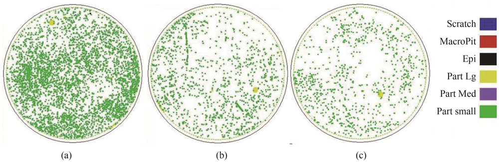
    Fig. 1. KLA-Tencor Candela particle metrology maps of the three InAs wafer surface treated by different wet cleaning processes(a)sample A,(b)sample B,and(c)sample C
    XPS spectra of wafer B and C,details of the binding energy given in Table 4
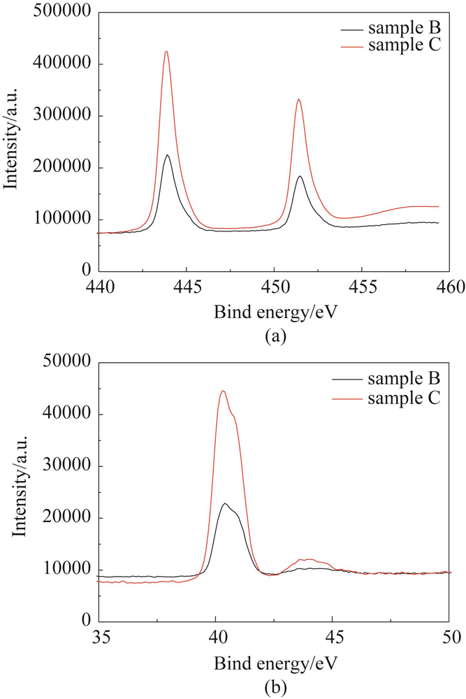
    Fig. 2. XPS spectra of wafer B and C,details of the binding energy given in Table 4
    Normarski microscope(a)sample B,and(b)sample C
    Fig. 3. Normarski microscope(a)sample B,and(b)sample C
    Hillocks defect from scanning electron microscopy after SL growth
    Fig. 4. Hillocks defect from scanning electron microscopy after SL growth
    Transmission electron microscope of hillocks defect
    Fig. 5. Transmission electron microscope of hillocks defect
    Sample No.Wet Chemical Cleaning Step
    ANH4OH∶H2O2∶H2O=1∶1∶10RinseDry
    BHC1∶H2O=1∶30RinseNH4OH∶H2O2∶H2O=1∶1∶10RinseDry
    CHC1∶H2O=1∶30RinseNH4OH∶H2O2∶H2O=1∶0.2∶10RinseDry
    Table 1. Multi-step wet cleaning processes used in this study
    Sample NoSiPSC1KCaTiCrMnFeNiCuZn
    A1 05104281 05744 5427 5530000000
    B494024454438 1293 7110001000
    C19707747838 1303 1640000000
    Table 2. TXRF results of the InAs wafer surface treated with different solution(1010 atoms/cm2
    SampleX/cmY/cmThickness/ÅAverage/Å
    Sample A01.515.1715.04
    1.5015.01
    0014.93
    -1.5015.07
    0-1.515.01
    Sample A01.510.2710.19
    1.5010.34
    0010.26
    -1.509.90
    0-1.510.18
    Sample A01.598.87
    1.508.9
    008.79
    -1.508.89
    0-1.58.78
    Table 3. Native oxide thickness measured by ellipsometer
    SampleIn3d(eV)As3d(eV)

    In/As

    Atomic percent

    In2O3InAsIn2O5As2O3AsInAs
    45144445.244.541.640.5
    B451.5444.0945.244.241.640.981.82%
    C451.4443.9345.144.141.340.670.61%
    Table 4. Binding energy of the peaks in XPS spectra and In/As Atomic percent of sample B and C
    Li-Jie LIU, You-Wen ZHAO, Yong HUANG, Yu ZHAO, Jun WANG, Ying-Li WANG, Gui-Ying SHEN, Hui XIE. Preparation of epi-ready InAs substrate surface for InAs/GaSb superlattice infrared detectors grown by MOCVD[J]. Journal of Infrared and Millimeter Waves, 2022, 41(2): 420
    Download Citation