1Key Laboratory of Semiconductor Materials Science,Beijing Key Laboratory of Low Dimensional Semiconductor Materials and Devices,Institute of Semiconductors,Chinese Academy of Sciences,Beijing 100083,China
2College of Materials Science and Opto-electronic Technology,University of Chinese Academy of Sciences,Beijing 100049,China
3Key Lab of Nanodevices and Applications,Suzhou Institute of Nano-Tech and Nano-Bionics,Chinese Academy of Sciences,Suzhou 215123,China
Total reflection X-ray fluorescence spectroscopy (TXRF) and X-ray photo-electron spectroscopy (XPS) have been used to investigate residual impurities and oxides on polished InAs substrate surface wet cleaned by different solution combination. Metal impurities Si, K and Ca are routinely detected on the cleaned InAs surface and their concentration change with the variation of solution combination. A large quantity of particles (80 nm size) is measured on the InAs substrate surface with higher residual impurity concentration. An effective wet chemical cleaning procedure is presented to prepare InAs substrate surface with less residual impurity, small particle quantity and thin oxide layer, which are beneficial to high quality epitaxial growth.
InAs is an important Ⅲ-Ⅴ semiconductors with narrow bandgap,high electron mobility and many applications in micro- and opto-electronic devices [1-2]. Especially,it is a useful substrate for InAs/GaSb Type-II superlattice infrared detectors due to a lattice constant of 6.054 Å nearly match to GaSb with 6.094 Å [3-5]. Generally,high quality of epitaxial growth and device strongly requires a good cleaning technique to achieve high-quality epi-ready InAs substrate surface foundation. Researchers have employed many experiments and established reviews that the alkaline solutions are accompanied by the removal of the part of particle and then the formation of a thin chemical oxide from Si and GaAs exactly [6-7]. For InP substrate,alkaline solution basically was used as predominantly chemical treatments and originally designed for Si and GaAs,which possess similarity to the material characterization [8-9]. Also some reports which require the addition of an acidic solution show this is not the case due to the difference oxide behavior between indium and gallium [10]. For InAs substrate,Some researchers treated InAs surfaces with sodium sulfide aqueous solutions in order to removal a natural oxide layer [11],some used a combination of HF:methanol wet etching followed by atomic hydrogen treatment to achieve the result of oxide removal[12],and some studied the kinetic between HCl and InAs through a quantitative analysis of the oxide formation [13]. However,InAs epi-ready substrate prior to epitaxial growth through surface characteristics(i.e. particle,residual impurities and nature oxide thickness)has not been studied extensively.
In this work,NH4OH,HCl and H2O2 based solutions were combined used with an aim to remove particle,residual impurities and leave a thin oxide layer on the substrate surface. Furthermore,an appropriate stoichiometric InAs surface were obtained in order to desorb easily during epitaxial growth process. With the help of TXRF,XPS,Scanning Electron Microscope(SEM)and surface scan measurement,an effective chemical cleaning procedure is presented for the preparation of high quality InAs epi-ready substrate.
1 Experimental
2-inch un-doped InAs wafers with(100)-orientation were sliced from an InAs(100)ingot grown in our laboratory by the liquid-encapsulated Czochralski(LEC)method[14-17]. The InAs wafers were lapped,polished,cleaned and packaged as epi-ready substrate in a class 100 cleaning room. During the final cleaning processing,different multi-step wet chemical cleaning processes were employed as listed in Table 1.
Sample No.
Wet Chemical Cleaning Step
A
NH4OH∶H2O2∶H2O=1∶1∶10
Rinse
Dry
B
HC1∶H2O=1∶30
Rinse
NH4OH∶H2O2∶H2O=1∶1∶10
Rinse
Dry
C
HC1∶H2O=1∶30
Rinse
NH4OH∶H2O2∶H2O=1∶0.2∶10
Rinse
Dry
Table 1. Multi-step wet cleaning processes used in this study
Three wet chemical cleaning processes were used to remove wafer contamination including particulate contamination,organic contamination and metallic contamination et al. Residual metal impurities on the wafer surface have been analyzed quantitatively by TXRF. The cleaned wafer surface defects,including particles,scratches,large pits,etc. were detected and classified using a KLA-Tencor Candela surface scanner. Nature oxide layer on the wafer surface was shown by an ellipsometer measurement. XPS is used to check oxide composition. Epitaxial defects morphology and formation are analyzed by SEM and Transmission electron microscopy(TEM),respectively.
2 Results and discussion
2.1 Residual metal impurities and particles
TXRF was used to detect and compare metal contamination on the wafer surface treated with different wet solutions. Table 2 demonstrate residual metal concentration on the InAs wafer surface cleaned with different solution combination.
Sample No
Si
P
S
C1
K
Ca
Ti
Cr
Mn
Fe
Ni
Cu
Zn
A
1 051
0
428
1 057
44 542
7 553
0
0
0
0
0
0
0
B
494
0
244
544
38 129
3 711
0
0
0
1
0
0
0
C
197
0
77
478
38 130
3 164
0
0
0
0
0
0
0
Table 2. TXRF results of the InAs wafer surface treated with different solution(1010 atoms/cm2)
NH4OH:H2O2:H2O based solution(SC1)are quite effective to remove particles and widely used in the wafer cleaning process of Si and GaAs substrates [6-7,10]. In this work,the solution(NH4OH:H2O2:H2O=1:1:10)is also proved to be effective in removing particles. In addition,metal impurities Ti,Cr,Mn,Fe,Ni,Cu,Zn on the InAs wafer is below the detection limitation. However,it is noted that alkali metals(K,Ca)and other elements(Si,S,Cl)remain at a very high concentration around 1014 atoms/cm2 on the wafer surface(sample A). It is necessary to further reduce the concentration of alkali metals to avoid their negative influence on the electrical property of InAs based epitaxial layer and device performance [18]. Dilute HCl solution is used to dissolve the metals because the charge exchange reaction is followed by ,metals transfer to ions and removed by DI water rinse. As shown in Table 1,the concentration of residual alkali metal on the surface of sample B is significantly lower after the cleaning process. Reduction of the H2O2 concentration in SC-1 by a factor of 5 has the effect to prevent micro-roughening of the InAs surface and to enhance metal particle removal. On the other hand,hydrogen peroxide in the solution has a higher oxidation potential and strong oxidation capacity. Compared with the high concentration of hydrogen peroxide in SC-1 solution,the lower solution possesses the weaker oxidability and the stronger complexation,therefore it is more conducive to the removal of metal ions. As a consequence,sample C has the lowest residual metal contamination among the three wafers treated by the different cleaning processes.
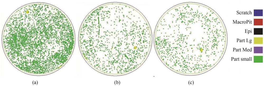
Figure 1 presents the KLA-Tencor Candela map metrology of particles on the InAs wafer treated by the three wet cleaning processes,respectively. Generally,the particle on the wafer has characteristic dimensions that can span several orders of magnitude,depending on the cleaning effect. For the three InAs wafer samples,most of the particles have size ranging from 0.08 µm to 0.15 µm(the detection limit of the instrument is 0.08 µm),as shown in the figure 1 labeled by green point. The total particle counts of the three sample wafers are 4428,1243 and 875,respectively,with 3-mm edge exclusion. Refer to the results given in Table 2,the variation trend of particle quantity correlates well with metal contamination concentration. This is reasonable since the particle itself must be consisted of impurities.
Figure 1.KLA-Tencor Candela particle metrology maps of the three InAs wafer surface treated by different wet cleaning processes(a)sample A,(b)sample B,and(c)sample C
As an epi-ready substrate for high quality epitaxial growth,the residual oxides on the InAs is of considerable importance. The surface of indium arsenide has a large number of indium or arsenic suspension bonds with an unsaturated state after chemical mechanical polishing. The arsenic dangling bond prior to indium dangling bond combines with oxygen atoms from the InAs substrate,forming As2O3 on substrate surface that will continue to react with InAs single crystal surface through chemical Eqs. 1-2. This causes large amounts of indium trioxide adhere to the wafer surface. In2O3 can be dissolved from the wafer surface via chemical reaction in HCl solution as shown in Eq. 3. Besides,a low dose of H2O2 from SC-1 in the final process can stop the formation of the indium oxide due to chemical reaction given by Eq. 4-5[19]. In this way,the thickness of the oxide on the wafer surface of sample C is quite small,as shown in the following results.
,
,
,
,
.
Table 3 shows the results of five points native oxide thickness,including the center and 4 positions around the center by 1.5-cm. To check the oxides thickness,ellipsometer measurement is conducted to compare oxide thickness on the wafer surface undergone the multi-step wet chemical cleaning process [20]. The nature oxide layer thicknesses are 15.04Å,10.19Å and 8.87Å,respectively. Sample B and sample C have lower native oxide thickness for HCl can dissolve the oxides effectively.
Sample
X/cm
Y/cm
Thickness/Å
Average/Å
Sample A
0
1.5
15.17
15.04
1.5
0
15.01
0
0
14.93
-1.5
0
15.07
0
-1.5
15.01
Sample A
0
1.5
10.27
10.19
1.5
0
10.34
0
0
10.26
-1.5
0
9.90
0
-1.5
10.18
Sample A
0
1.5
9
8.87
1.5
0
8.9
0
0
8.79
-1.5
0
8.89
0
-1.5
8.78
Table 3. Native oxide thickness measured by ellipsometer
Moreover,a substrate wafer with stoichiometric thin oxide layer,less particle and low residual impurity concentration is highly high quality epi-growth. In order to clarify the chemical composition of oxides on the InAs wafer surface from sample B and sample C,XPS was used to analyze the core level and valence-band spectra of the oxides,as shown in Fig. 2. Binding energies and energy separation,for core levels,are presented in table 4. Due to charging effects,absolute binding energies are given with a deviation of ±0.3 eV[21]. By verifying the binding energy values some parameters can be determined for the identification of oxide composition.
Figure 2.XPS spectra of wafer B and C,details of the binding energy given in Table 4
From the measured results,it is able to distinguish the existed oxide from particular shapes of In3s and As3d spectra. Compounds In2O3,As,As2O3 and As2O5 were identified according to the specific binding energy. By calculating the peak intensity area ratio of indium and arsenic,the atomic ration of indium and arsenic are 0.8182 and 0.7061 for sample B and sample C,respectively. This result suggests that sample C has more arsenic rich oxide than sample B on its surface.
2.3 Epitaxial results
On the preparation InAs substrates of sample B and sample C,a 200 nm n+ LWSL bottom contact,an LWSL absorber of 2 µm thickness,a MWSL barrier of 200 nm and another 200 nm-thick p-MWSL contact were deposited in the same run by an Aixtron 2400G3 MOCVD growth system. Details on epitaxial design and growth are described in Ref.[22]. The defect density of epitaxial surface is observed by a Normarski(Fig. 3). The epitaxial defect density from sample B is 990/cm2(Fig. 3(a)),while 140/cm2 is from sample C(Fig. 3(b)). The defect in morphology look like hillocks with about 9 µm×6 µm,which is obtained by a scanning electron microscopy analyses,as shown in Fig. 4. A TEM sample was prepared by using a focused ion beam. TEM(Fig. 5)showed that there was a bulge at the interface between substrate and epitaxial. This bulge forms the center of the defect source,causing epitaxial growth stress in the epitaxial layer. This little bump could be a particle,a residue metal impurity,or indium oxide without complete desorption from nature oxide. Therefore,it is reasonable that the sample B with more residual metal impurities and particles,thicker nature oxide thickness and rich indium surface has more defects density.
Figure 3.Normarski microscope(a)sample B,and(b)sample C
HCl-based solution,combined with SC1 is beneficial for the reduction of particles and metals on InAs wafer surface. Lower concentration of H2O2 in the NH4OH mixture produces thinner oxide and arsenic-rich oxide surface. InAs wafer with thin oxide and arsenic-rich oxide surface is good to high quality epitaxial growth. The lower defect density of 140/cm2 from SL by MOCVD is obtained through InAs substrate treatment technique.
[17] X Lu, Y Zhao, W Sun et al. Lattice perfection of GaSb and InAs single crystal substrate. Pan Tao Ti Hsueh Pao/Chinese Journal of Semiconductors, 28, 163-166(2007).