• Journal of Semiconductors
  • Vol. 41, Issue 10, 102402 (2020)
Chenxia Wang, Jie Wei, Diao Fan, Yang Yang, and Xiaorong Luo
Author Affiliations
  • China State Key Laboratory of Electronic Thin Films and Integrated Devices, University of Electronic Science and Technology of China, Chengdu 610054, China
  • show less
    DOI: 10.1088/1674-4926/41/10/102402 Cite this Article
    Chenxia Wang, Jie Wei, Diao Fan, Yang Yang, Xiaorong Luo. A snapback-free and high-speed SOI LIGBT with double trenches and embedded fully NPN structure[J]. Journal of Semiconductors, 2020, 41(10): 102402 Copy Citation Text show less
    (Color online) Schematic cross-sectional views of (a) DT-NPN LIGBT, (b) SEG LTIGBT, and (c) SSA LTIGBT.
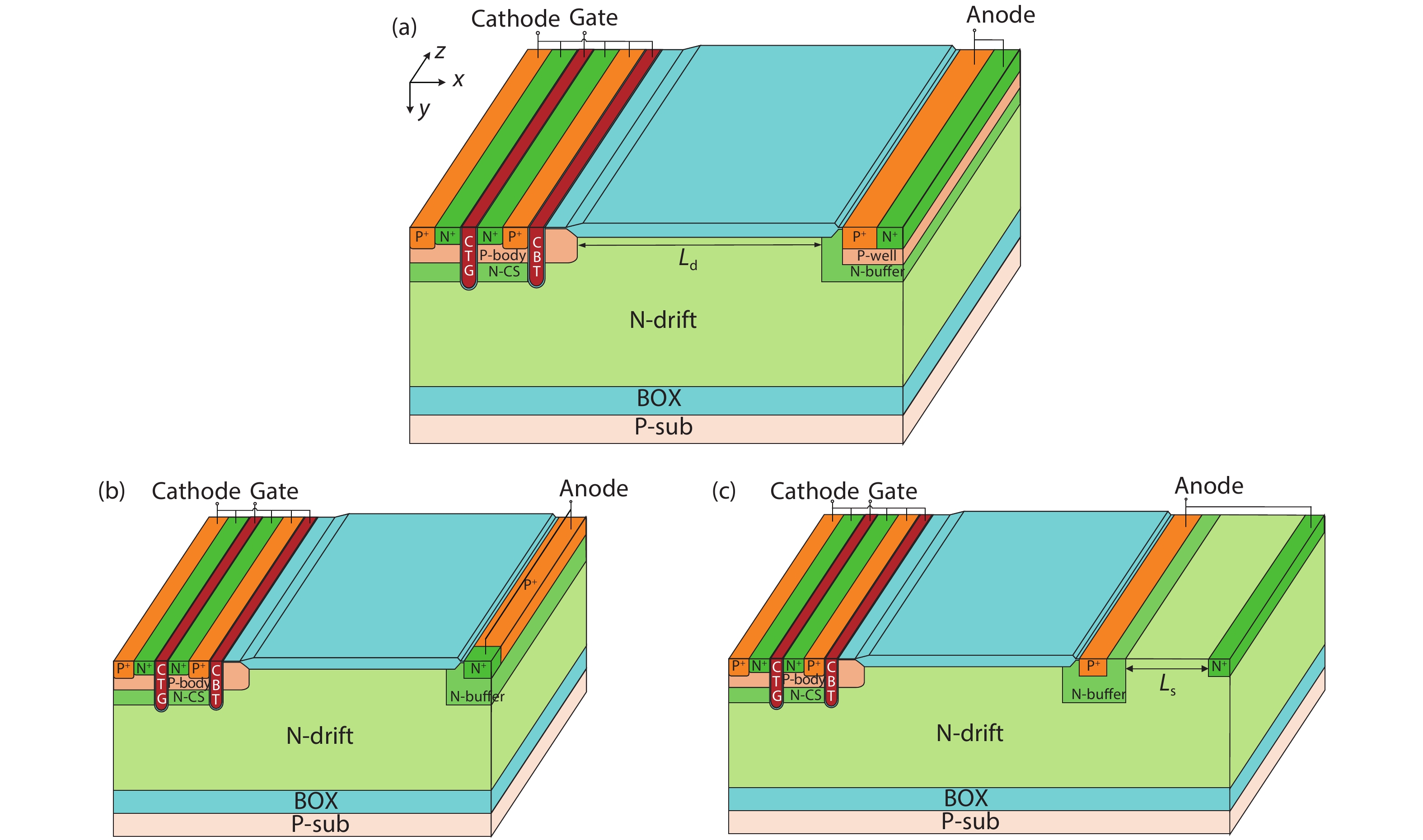
    Fig. 1. (Color online) Schematic cross-sectional views of (a) DT-NPN LIGBT, (b) SEG LTIGBT, and (c) SSA LTIGBT.
    (Color online) Equivalent circuit of the DT-NPN LIGBT. Rp-body and Rp are distributed resistance at the cathode and anode region, respectively.
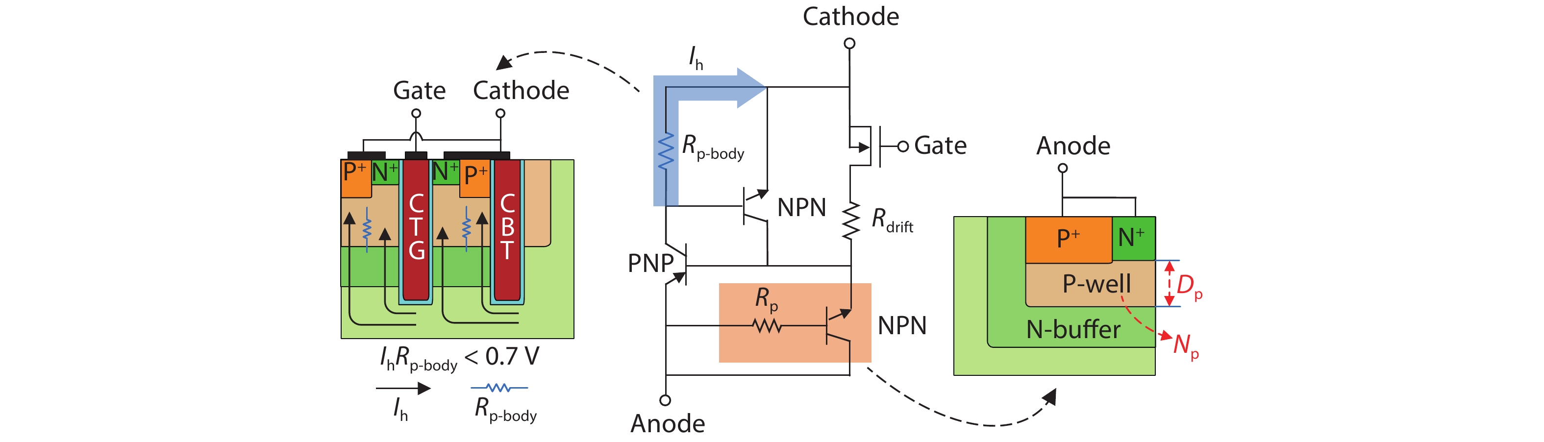
    Fig. 2. (Color online) Equivalent circuit of the DT-NPN LIGBT. Rp-body and Rp are distributed resistance at the cathode and anode region, respectively.
    (Color online) (a) Dependences of the BV and Von on NA. (b) Breakdown characteristics. Here Ie and Ih represent the electron current and hole current, respectively.
    Fig. 3. (Color online) (a) Dependences of the BV and Von on NA. (b) Breakdown characteristics. Here Ie and Ih represent the electron current and hole current, respectively.
    (Color online) Snapback characteristics for different devices. Wp/Wn is the width of P+/N+ anode. ΔVSB is snapback voltage.
    Fig. 4. (Color online) Snapback characteristics for different devices. Wp/Wn is the width of P+/N+ anode. ΔVSB is snapback voltage.
    (Color online) Total current density distribution and the flowlines for (a) the proposed LIGBT (at point A in Fig. 4), (b) the SEG LTIGBT (at point C in Fig. 4), and (c) the SSA LTIGBT (at point B in Fig. 4).
    Fig. 5. (Color online) Total current density distribution and the flowlines for (a) the proposed LIGBT (at point A in Fig. 4), (b) the SEG LTIGBT (at point C in Fig. 4), and (c) the SSA LTIGBT (at point B in Fig. 4).
    (Color online) Influences of the Np and Dp on (a) forward conduction characteristics at VG = 15 V, (b) conduction energy band distribution of P-well/N-buffer junction in the y-direction and (c) ΔVSB, Von and Eoff. qψH and WH are the height and width of electron barrier. To entirely suppress the snapback by optimizing the Np and Dp, the qψH is about 0.75 eV.
    Fig. 6. (Color online) Influences of the Np and Dp on (a) forward conduction characteristics at VG = 15 V, (b) conduction energy band distribution of P-well/N-buffer junction in the y-direction and (c) ΔVSB, Von and Eoff. H and WH are the height and width of electron barrier. To entirely suppress the snapback by optimizing the Np and Dp, the H is about 0.75 eV.
    (Color online) Forward conduction characteristics. Insets: hole density distribution for different LIGBTs at the cathode side (@ y = 4.1 μm) and schematic cross-sectional views of four different cathode structures for LIGBTs with the same anode structure as that of the proposed DT-NPN LIGBT.
    Fig. 7. (Color online) Forward conduction characteristics. Insets: hole density distribution for different LIGBTs at the cathode side (@ y = 4.1 μm) and schematic cross-sectional views of four different cathode structures for LIGBTs with the same anode structure as that of the proposed DT-NPN LIGBT.
    (Color online) Switching characteristics: (a) switching waves, the inset shows the simulation circuit with RG = 10 Ω and LS = 10 nH, (b) carrier distribution at different time, (c) current flowlines through the embedded NPN structure at t3.
    Fig. 8. (Color online) Switching characteristics: (a) switching waves, the inset shows the simulation circuit with RG = 10 Ω and LS = 10 nH, (b) carrier distribution at different time, (c) current flowlines through the embedded NPN structure at t3.
    (Color online) IA–VA characteristics for the DT-NPN and MSA LIGBT.
    Fig. 9. (Color online) IAVA characteristics for the DT-NPN and MSA LIGBT.
    (Color online) Eoff–Von tradeoff of different LIGBTs.
    Fig. 10. (Color online) EoffVon tradeoff of different LIGBTs.
    (Color online) Key fabrication steps. (a) N-buffer and N-CS-layer implantations. (b) P-well and P-body implantations. (c) Trenches etching, oxidation, and poly-silicon deposition. (d) Implantations for N+/P+ regions and formation of metal contacts.
    Fig. 11. (Color online) Key fabrication steps. (a) N-buffer and N-CS-layer implantations. (b) P-well and P-body implantations. (c) Trenches etching, oxidation, and poly-silicon deposition. (d) Implantations for N+/P+ regions and formation of metal contacts.
    ParameterDT-NPNSEGSSA
    N-drift length, Ld (μm) 545454
    SOI layer thickness, Ts (μm) 252525
    Buried oxide thickness, tbox (μm) 333
    N-drift doping, Nd (1014 cm−3) 222
    N-buffer doping, Nbuffer (1016 cm−3) 626
    N-CS doping, Ncs (1016 cm−3) 666
    P-body doping, Np-body (1017 cm−3) 111
    Gate oxide thickness (μm) 0.10.10.1
    Trench depth (μm) 444
    Table 1. Key parameters for LIGBTs.
    Chenxia Wang, Jie Wei, Diao Fan, Yang Yang, Xiaorong Luo. A snapback-free and high-speed SOI LIGBT with double trenches and embedded fully NPN structure[J]. Journal of Semiconductors, 2020, 41(10): 102402
    Download Citation