• Photonics Research
  • Vol. 10, Issue 1, 76 (2022)
Yanxian Wei1, Hailong Zhou1、4, Yuntian Chen1, Yunhong Ding2、3, Jianji Dong1、*, and Xinliang Zhang1
Author Affiliations
  • 1Wuhan National Laboratory for Optoelectronics, School of Optical and Electronic Information, Huazhong University of Science and Technology, Wuhan 430074, China
  • 2Department of Photonics Engineering, Technical University of Denmark, 2800 Lyngby, Denmark
  • 3SiPhotonIC ApS, 2830 Virum, Denmark
  • 4e-mail: hailongzhou@hust.edu.cn
  • show less
    DOI: 10.1364/PRJ.444075 Cite this Article Set citation alerts
    Yanxian Wei, Hailong Zhou, Yuntian Chen, Yunhong Ding, Jianji Dong, Xinliang Zhang. Anti-parity-time symmetry enabled on-chip chiral polarizer[J]. Photonics Research, 2022, 10(1): 76 Copy Citation Text show less
    Concept and scheme of the chiral polarizer. (a) Comparison between conventional polarizer and our chiral polarizer. (b) Scheme of our chiral polarizer. The chiral polarizer is constructed with three waveguides WG1, WG2, and WG3; where WG1 and WG3 are supposed to be lossless, and WG2 has a high loss. (c) Encircling EP evolution clockwise. (d) Encircling EP evolution counterclockwise.
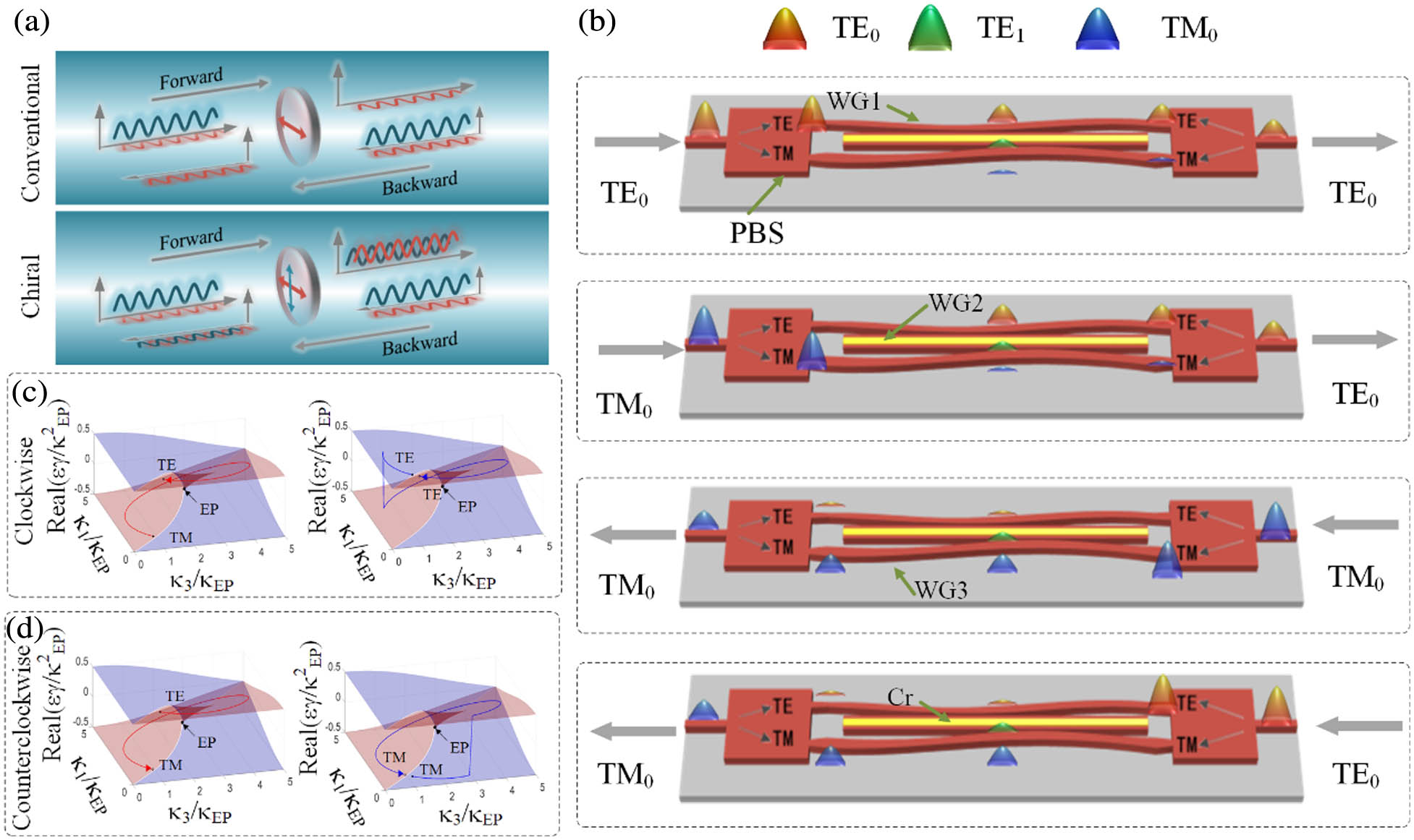
    Fig. 1. Concept and scheme of the chiral polarizer. (a) Comparison between conventional polarizer and our chiral polarizer. (b) Scheme of our chiral polarizer. The chiral polarizer is constructed with three waveguides WG1, WG2, and WG3; where WG1 and WG3 are supposed to be lossless, and WG2 has a high loss. (c) Encircling EP evolution clockwise. (d) Encircling EP evolution counterclockwise.
    Detailed design of chiral polarizer. (a) Effective refractive index of each mode versus the width of waveguide. (b) Optimized gap transform function that generates encircling EP parametric evolution. (c) Wavelength-dependent parametric loops for the design shown in (a) and (b).
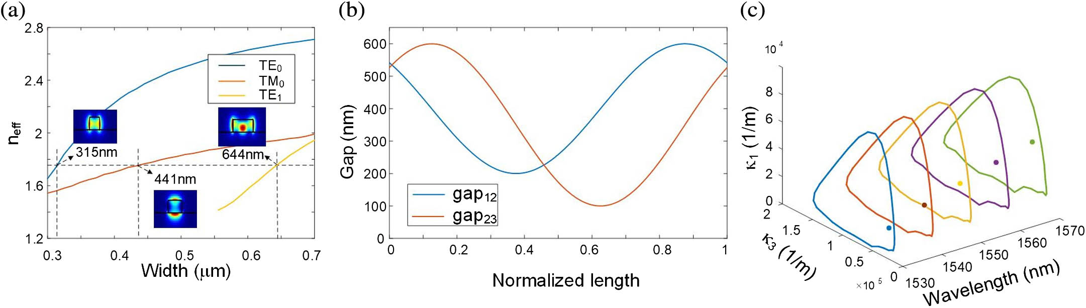
    Fig. 2. Detailed design of chiral polarizer. (a) Effective refractive index of each mode versus the width of waveguide. (b) Optimized gap transform function that generates encircling EP parametric evolution. (c) Wavelength-dependent parametric loops for the design shown in (a) and (b).
    Simulation results of the chiral polarizer. (a) Simulation power distributions in the waveguides for forward and backward propagation. (b) Transmission spectra for different input.
    Fig. 3. Simulation results of the chiral polarizer. (a) Simulation power distributions in the waveguides for forward and backward propagation. (b) Transmission spectra for different input.
    SEM images of the chip and the experimentally measured spectra. (a) SEM images of the proposed chiral polarizer. Zoom-in images of polarization beam splitter and coupled region are shown in the subgraphs. (b)–(e) Experimentally measured spectra of the device for the (b), (c) forward propagation and (d), (e) backward propagation. TE and TM denote the modes input or output from the left; TE’ and TM’ denote the modes input or output from the right. (f), (g) Test results of the PBS.
    Fig. 4. SEM images of the chip and the experimentally measured spectra. (a) SEM images of the proposed chiral polarizer. Zoom-in images of polarization beam splitter and coupled region are shown in the subgraphs. (b)–(e) Experimentally measured spectra of the device for the (b), (c) forward propagation and (d), (e) backward propagation. TE and TM denote the modes input or output from the left; TE’ and TM’ denote the modes input or output from the right. (f), (g) Test results of the PBS.
    Experiment setup and results of communication experiment. (a) Experiment setup. (b) The 10 GHz OOK bits stream loaded on TE and TM modes for inputting forward. (c) Power summary of the output TE and TM modes. (d), (e) Result of inputting backward. TE and TM denote the input or output modes from the left; TE’ and TM’ denote the input or output modes from the right.
    Fig. 5. Experiment setup and results of communication experiment. (a) Experiment setup. (b) The 10 GHz OOK bits stream loaded on TE and TM modes for inputting forward. (c) Power summary of the output TE and TM modes. (d), (e) Result of inputting backward. TE and TM denote the input or output modes from the left; TE’ and TM’ denote the input or output modes from the right.
    Yanxian Wei, Hailong Zhou, Yuntian Chen, Yunhong Ding, Jianji Dong, Xinliang Zhang. Anti-parity-time symmetry enabled on-chip chiral polarizer[J]. Photonics Research, 2022, 10(1): 76
    Download Citation