Peili Zhao, Lei Li, Guoxujia Chen, Xiaoxi Guan, Ying Zhang, Weiwei Meng, Ligong Zhao, Kaixuan Li, Renhui Jiang, Shuangfeng Jia, He Zheng, Jianbo Wang. Structural evolution of low-dimensional metal oxide semiconductors under external stress[J]. Journal of Semiconductors, 2022, 43(4): 041105
Search by keywords or author
- Journal of Semiconductors
- Vol. 43, Issue 4, 041105 (2022)
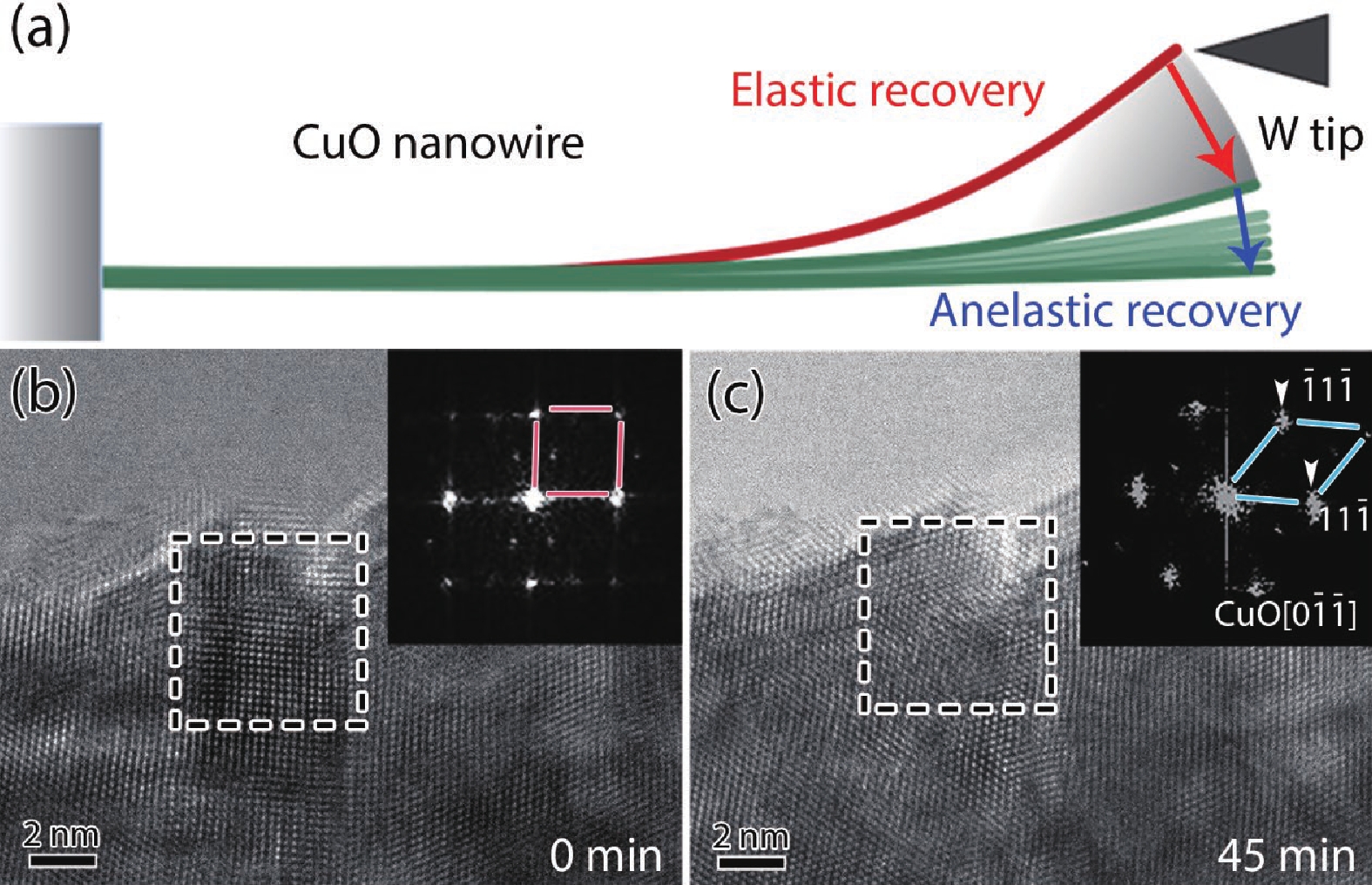
![(Color online) Anelasticity in CuO induced by the point defects migration[69]. (a) Schematic illustration of the anelastic deformation process. (b) High-resolution TEM (HRTEM) image showing the nucleation of CuO0.67 phase (enclosed area), indicated by the inserted fast Fourier transform (FFT) pattern. (c) The reversible transition from CuO0.67 to CuO after the compressive stress released.](/richHtml/jos/2022/43/4/041105/img_1.jpg)
Fig. 1. (Color online) Anelasticity in CuO induced by the point defects migration[69 ]. (a) Schematic illustration of the anelastic deformation process. (b) High-resolution TEM (HRTEM) image showing the nucleation of CuO0.67 phase (enclosed area), indicated by the inserted fast Fourier transform (FFT) pattern. (c) The reversible transition from CuO0.67 to CuO after the compressive stress released.
![(Color online) Oxygen vacancy diffusion pathways in CuO[69]. (a) The high-angle annular dark field (HAADF) showing lattice planes of CuO and metastable CuO0.67 phases. (b –d) Three possible diffusion pathways of O vacancies in CuO. The brown and blue spheres depict O and Cu atoms, respectively.](/richHtml/jos/2022/43/4/041105/img_2.jpg)
Fig. 2. (Color online) Oxygen vacancy diffusion pathways in CuO[69 ]. (a) The high-angle annular dark field (HAADF) showing lattice planes of CuO and metastable CuO0.67 phases. (b –d) Three possible diffusion pathways of O vacancies in CuO. The brown and blue spheres depict O and Cu atoms, respectively.
Fig. 3. (Color online) The phase transition of ZnO NW with
81 ]. (a–c) The HAADF images showing the atomistic phase transition of ZnO NW. (d–f) The enlarged view of the regions indicated by the blue rectangles in (a–c), respectively. (g–i) MD simulation results mirror the phase transition pathway observed in the experiments showing the reversible phase transitions. The red and grey spheres depict O and Zn atoms, respectively.
Fig. 4. (Color online) The phase stability of WZ, h-MgO, and BCT structures in ZnO[81 ]. (a) The cross-sectional view of ZnO showing the bond formation and breaking during the phase transition (“○” represents the bond formation of Zn–O, “×” represents the bond breaking of Zn-O). (b) The phase diagram related to the width and thickness of the NWs under 0% and 7% strain. The red and grey spheres depict O and Zn atoms, respectively.
Fig. 5. (Color online) The effects of e-beam irradiation on the anelasticity in CuO NWs[27 , 69 ]. (a–d) TEM images showing the anelastic strain recovery with e-beam illumination. (e–h) TEM images showing the anelastic strain recovery of the same CuO NW without e-beam. The images were taken every 10 seconds. (i) Curves showing the anelastic strain as a function of time.
Fig. 6. The phase transition of ZnO NW by applying 200 kV e-beam[81 ]. (a–c) HRTEM images showing the real-time atomistic phase transition process of ZnO NW with the axial direction of

Set citation alerts for the article
Please enter your email address


