
Bo Wang, Liheng Wang, Weixin Liu, Zebin Kong, Yudong Li, Zhen Li, Kunshu Wang, Weiming Zhu, Ming Xuan. Single-Event Upset and Damage Mechanism in 8T-Global Shutter CMOS Image Sensors[J]. Acta Optica Sinica, 2019, 39(5): 0504001
- Acta Optica Sinica
- Vol. 39, Issue 5, 0504001 (2019)
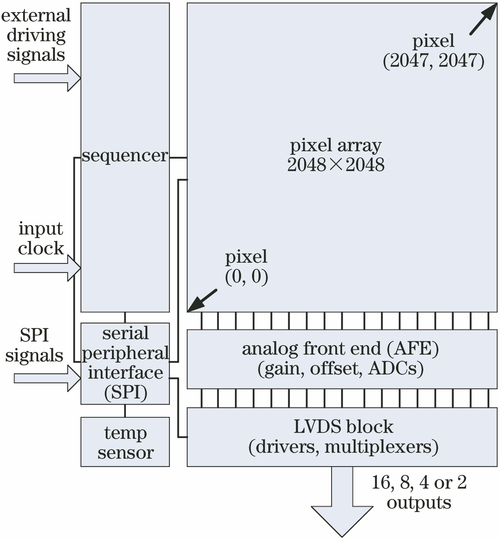
Fig. 1. Block diagram of CMV4000 image sensor
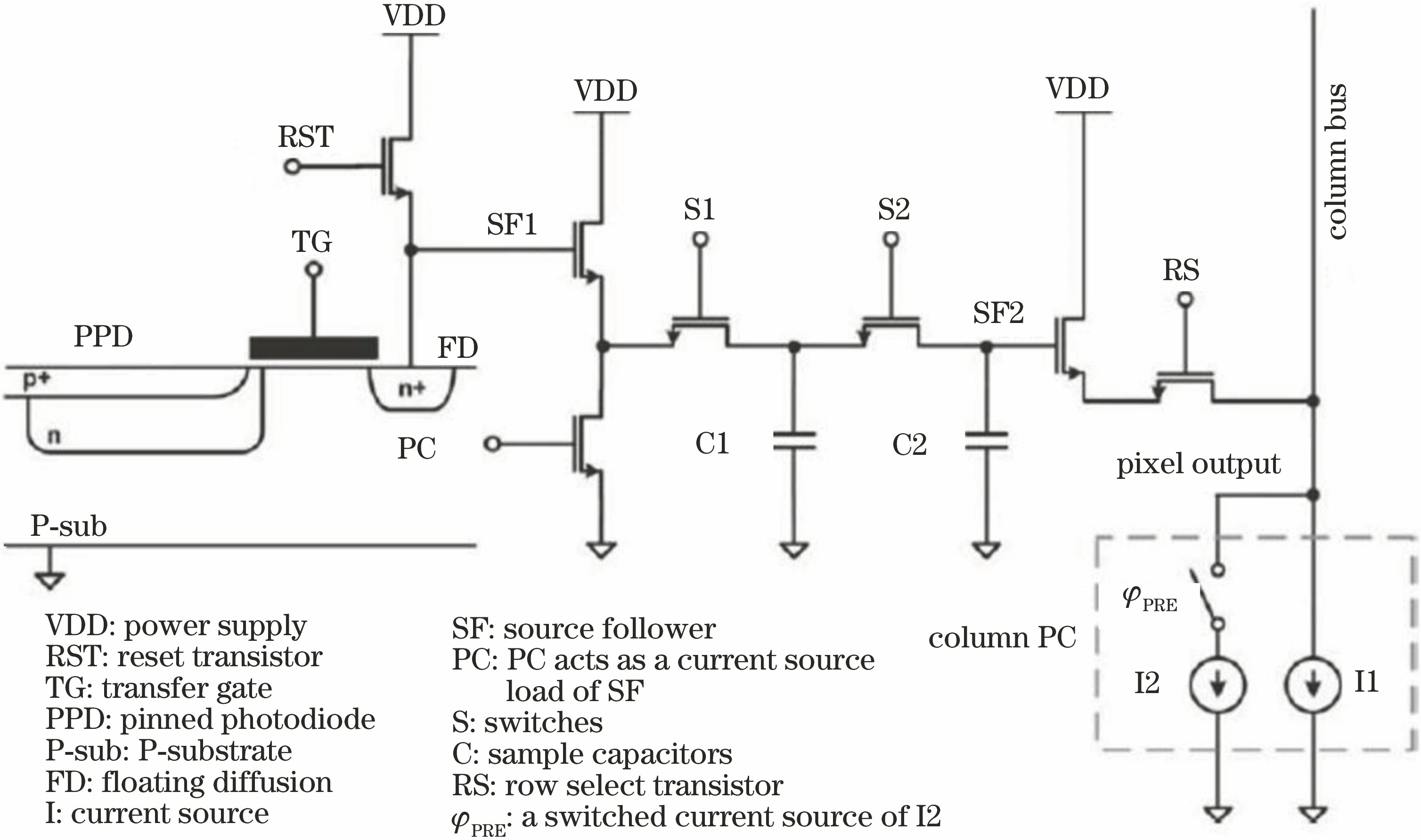
Fig. 2. Cross-sectional diagram of 8T pixel unit
Fig. 3. SEU diagram of standard 6T structure SRAM storage unit after exposure to heavy-ion irradiation[13]
Fig. 4. Block diagram of 8T-global exposure CIS single-particle online detection system
Fig. 5. Abnormal images after SEU in offset register. (a) Nth; (b) (N+1)th; (c) (N+2)th
Fig. 6. Three-dimensional stereograms of image abnormal mode after SEU in offset register. (a) Nth; (b) (N+1)th; (c) (N+2)th
Fig. 7. Image abnormal mode after SEU in LVDS output register
Fig. 8. Image abnormal mode after SEU in row-decoder address decoder
Fig. 9. Image abnormal mode after SEU in output clock register
Fig. 10. Working diagram of 8-channel LVDS. (a) Reading out line by line for LVDS; (b) pixel output line coordinate corresponding to each LVDS
Fig. 11. Timing diagram of 10-bit pixel output
Fig. 12. Schematic of corrupted code for 10-bit pixel output
|
Table 1. Ion information for heavy-ion irradiation tests
|
Table 2. CIS SEU test data
|
Table 3. Image abnormal modes caused by SEU
|
Table 4. Original setting of CMV4000 offset register

Set citation alerts for the article
Please enter your email address
© Copyright 2018-2021 | Chinese Laser Press. All Rights Reserved 沪ICP备15018463号-20