• Journal of Semiconductors
  • Vol. 40, Issue 6, 061003 (2019)
Hongtao Ren1、2, Yachao Liu1, Lei Zhang1, and Kai Liu2
Author Affiliations
  • 1MOE Key Laboratory for Nonequilibrium Synthesis and Modulation of Condensed Matter, School of Science, Xi’an Jiaotong University, Xi’an 710049, China
  • 2State Key Laboratory of New Ceramics and Fine Processing, School of Materials Science and Engineering, Tsinghua University, Beijing 100084, China
  • show less
    DOI: 10.1088/1674-4926/40/6/061003 Cite this Article
    Hongtao Ren, Yachao Liu, Lei Zhang, Kai Liu. Synthesis, properties, and applications of large-scale two-dimensional materials by polymer-assisted deposition[J]. Journal of Semiconductors, 2019, 40(6): 061003 Copy Citation Text show less
    (Color online) Timeline showing key development by polymer-assisted deposition. Metal oxides; metal nitrides; metal carbides; glassy-graphene; MoS2; MoS2/glassy-graphene heterostructure.
    Fig. 1. (Color online) Timeline showing key development by polymer-assisted deposition. Metal oxides; metal nitrides; metal carbides; glassy-graphene; MoS2; MoS2/glassy-graphene heterostructure.
    (Color online) Application of as-grown thin films by PAD.
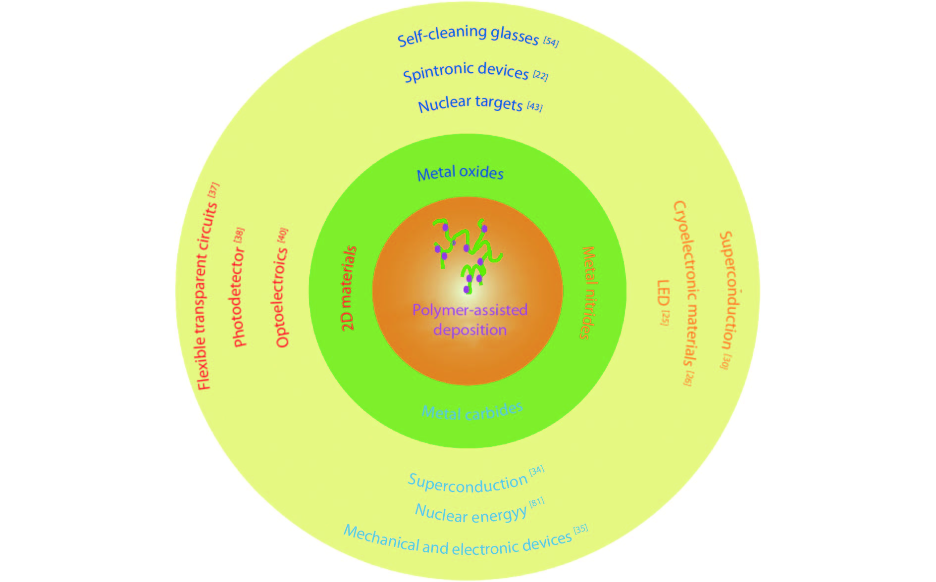
    Fig. 2. (Color online) Application of as-grown thin films by PAD.
    (Color online) Schematic illustration of the main processing steps used to grow thin films by PAD.
    Fig. 3. (Color online) Schematic illustration of the main processing steps used to grow thin films by PAD.
    (Color online) Evolution from glassy carbon to glassy-graphene and graphene[37].
    Fig. 4. (Color online) Evolution from glassy carbon to glassy-graphene and graphene[37].
    (Color online) Preparation of glassy graphene-based circuits and the flexibility test[37].
    Fig. 5. (Color online) Preparation of glassy graphene-based circuits and the flexibility test[37].
    (Color online) Thickness-dependent bandgap tunable MoS2 thin films for optoelectronics[40].
    Fig. 6. (Color online) Thickness-dependent bandgap tunable MoS2 thin films for optoelectronics[40].
    (Color online) Wafer-scale synthesis of MoS2 thin films via polymer-assisted deposition[39].
    Fig. 7. (Color online) Wafer-scale synthesis of MoS2 thin films via polymer-assisted deposition[39].
    (Color online) Formation of large-area web buckles[16].
    Fig. 8. (Color online) Formation of large-area web buckles[16].
    (Color online) Schematic of MGH preparation and 3D view of the transparent photodetector, photoresponsivity and time-resolved photoresponse of photodetectors under different illuminations[38].
    Fig. 9. (Color online) Schematic of MGH preparation and 3D view of the transparent photodetector, photoresponsivity and time-resolved photoresponse of photodetectors under different illuminations[38].
    Table 1. Elements in the magenta boxes coordinated with polymer to form a stable complex. The elements shown in red font were bound with the polymer in the previous reports.
    ElementMetal precursorPolymerElementMetal precursorPolymer
    Li[70]LiNO3PEI + EDTARu[49]RuCl3PAA
    C[37]C6H12O6PEIAg[84]AgNO3PEI + C6H8O7
    Al[68]Al(NO3)3PEI + HFIn[85]In(NO3)3PEI
    Ca[45]Ca(OH)2PEISn[86]SnCl2PEIC
    Sc[73]Sc(NO3)3PEI + EDTABa[65]Ba(NO3)2PEI + EDTA
    Ti[1]Ti(cat)3(NH4)2PEIHf[42]HfCl4PEI
    V [10]VOSO4PEI + EDTATa[33]TaCl5PEI + HF
    Mn[45]MnCl2PEI + EDTAW[87](NH4)2WO4PEI
    Fe[88]FeCl3PEIBi[10]Bi(NO3)3PEI + EDTA
    Co[88]CoCl2PEILa[45]La(NO3)3PEI + EDTA
    Ni[51]Ni(NO3)2PEI + EDTACe[72]Ce(NO3)3PEI + EDTA
    Cu[68]Cu(NO3)2PEIPr[76]Pr(NO3)3PEI + EDTA
    Zn[22]Zn(NO3)2PEINd[76]Nd(NO3)3PEI + EDTA
    Ga[25]GaCl5PEISm[76]Sm(NO3)3PEI + EDTA
    Ge[36]GeO2PEI + EDTAEu[42]EuCl3PEI
    Sr[1]Sr(NO3)2PEI + EDTAGd[72]Gd(NO3)3PEI + EDTA
    Y[10]Y(NO3)3PEI + EDTATm[42]TmCl3PEI
    Zr[55]ZrO(NO3)2PEI + EDTAU[89]UO2(oAc)2PEI
    Nb[26]NbCl5PEI + HFNp[46]239Np solution PEI + EDTA
    Mo[16](NH4)6Mo7O24PEI + EDTAPu[46]239Pu solution PEI + EDTA
    Table 2. Summary of various metal elements binded by polymers.
    MethodPrecursor gasTemperature (°C)CrystalizationConformalSizeMobility (cm2/(V·s)) Response timeIon/Ioff ratio
    CVDAr1000Single-crystalNo~cm29.6105[92]
    Ar850Single-crystalNo50106[92]
    ALDH2S; Ar 60AmorphousYes0.23102[93]
    PADAr + H2850PolycrystallineYes~cm20.3 ms3[40]
    Ar + H2700PolycrystallineYes6-inch1.0 ms104[39]
    Ar + H2550AmorphousYes~cm2[16]
    Table 3. Comparison of three different methods to synthesize MoS2 and MoS2 field-effect transistor structures.
    Hongtao Ren, Yachao Liu, Lei Zhang, Kai Liu. Synthesis, properties, and applications of large-scale two-dimensional materials by polymer-assisted deposition[J]. Journal of Semiconductors, 2019, 40(6): 061003
    Download Citation