
Enqing Zhang, Zhengkun Xing, Dian Wan, Haoran Gao, Yingdong Han, Yisheng Gao, Haofeng Hu, Zhenzhou Cheng, Tiegen Liu. Surface-enhanced Raman spectroscopy chips based on two-dimensional materials beyond graphene[J]. Journal of Semiconductors, 2021, 42(5): 051001
- Journal of Semiconductors
- Vol. 42, Issue 5, 051001 (2021)
Abstract
1. Introduction
Since it was originally discovered in the 1970s[
Two-dimensional (2D) materials provide us with emerging opportunities in SERS, since the discovery of graphene in 2004[
In this review, we comprehensively summarize novel SERS techniques based on metal-free 2D materials beyond graphene, including TMDs, BP, h-BN, and MXenes. Firstly, we briefly introduce 2D materials’ physicochemical properties, before categorizing the cutting-edge progress of SERS studies based on these substrates. Due to this paper’s length limit, SERS studies of metal-2D-material hybrid substrates are not included here. Finally, we summarize the review, and discuss prospects in this area. We hope this review will serve as a useful reference for researchers in the fields of 2D materials, spectroscopy, and their applications in chemical and biological sensing.
2. Mechanisms of SERS
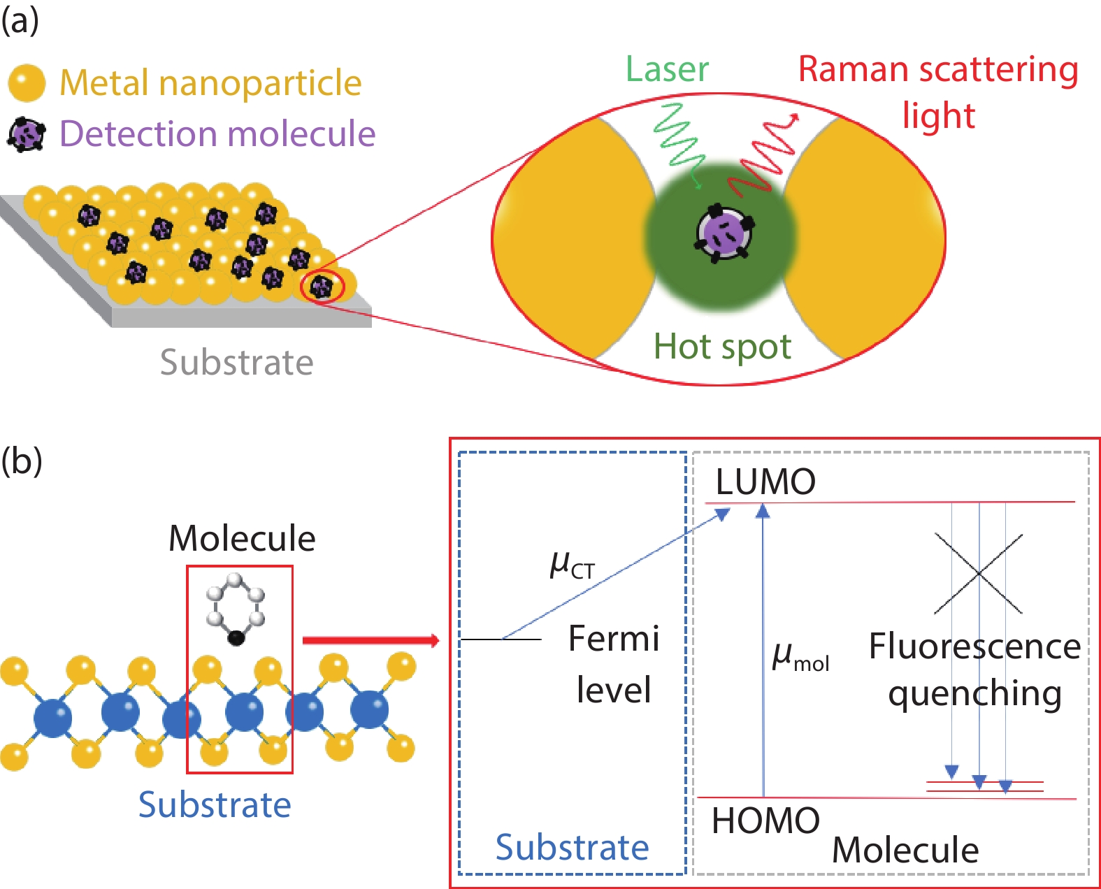
It is generally believed that the Raman enhancement in SERS originates primarily from two mechanisms: EMs and CMs. With respect to EMs, the Raman enhancement usually occurs around surface locations in noble metal nanoparticles, known as “hot spots”[
![]()
Figure 1.(Color online) Schematics of the mechanisms of SERS. (a) With respect to EMs, when the incident laser is in resonance with the nanoparticle LSPR frequency, the incident laser excites electrons on the metal surface, leading to a polarization of charge and oscillating dipoles. As the frequencies of Raman scattering light are close to that of the incident laser, the resonance also increases the intensity of the Raman scattering light. (b) For CMs, electrons are transferred from the Fermi level of the substrate to the LUMO of the molecule, thereby forming a charge transfer intermediate. The energy transition (
where
On the other hand, CMs are often attributed to the charge transfer effect, which is not yet clearly understood[
3. SERS based on 2D materials beyond graphene
In this section, we summarize SERS advances based on diverse 2D materials beyond graphene, as shown in Fig. 2. The section is divided into five parts, covering the development of SERS chips based on TMDs, h-BNs, BP, MXenes, and their heterostructures, respectively. In each part, we first briefly introduce the physiochemical properties of 2D materials for use in developing SERS, then discuss state-of-the-art experimental results.
![]()
Figure 2.(Color online) Comparison of various 2D materials beyond graphene for SERS applications, including TMDs, BP, h-BN, MXenes, and their heterostructures.
3.1. SERS based on TMDs
TMDs, consisting of covalently bonded X–M–X atoms (M = transition metals of groups IV–VI; X = chalcogen), where M is a transition metal atom (e.g., Mo or W), and X is a chalcogenide atom (e.g., S, Te or Se), have a series of superior properties, ideal for potential use in SERS chips[
Given these excellent properties, TMDs have been extensively studied for use in SERS chips[
![]()
Figure 3.(Color online) SERS studies based on TMDs. (a) Schematic of measurement and enhanced Raman spectra of 4-mercaptopyridine on monolayer MoS2. (b) Energy levels of the oxygen-incorporation MoS2-R6G system. Here,
3.2. SERS based on h-BN
h-BN, sp2-hybridized 2D insulator is a structural analog of graphene, with sublattices being occupied by equal numbers of boron and nitrogen atoms, arranged alternately in a honeycomb configuration[
Based on these unique properties, h-BN may be a good alternative to graphene for the purpose of Raman enhancement. It has been proposed that the Raman enhancement mechanism for h-BN may stem from different factors. In 2014, Ling et al.[
![]()
Figure 4.(Color online) SERS studies based on h-BN, BP, and MXenes. (a) Preparation of SERS chips based on graphene, h-BN, and MoS2. The layered 2D materials are shown in gray, while probe molecules are shown in red. (b) Raman spectra of CuPc molecules on SiO2/Si (black line), MoS2 (green line), h-BN (red line), and graphene (blue line) substrates. (c) Raman spectra of RhB molecules (~10–8 M) on a BP substrate, showing different Raman peaks, which could be attributed to different vibrational transitions in the RhB molecules. (d) Schematic of Ti2NT
3.3. SERS based on BP
Of all the 2D materials, BP demonstrates a series of unique characteristics for use in Raman enhancement. Firstly, BP, as a 2D layered material with anisotropy, can provide detailed information about the charge-transfer process as compared to the use of isotropic materials[
To explore the intrinsic SERS performance of BP[
3.4. SERS based on MXenes
MXenes share a general formula of Mn+1XnTx(n = 1–3), where M is an early transition metal, X is a carbon or nitrogen, and T is the surface termination (O, OH, F, or Cl)[
For their proof-of-the-concept, Ye et al.[
3.5. SERS based on 2D-material heterostructures
Recently, 2D van der Waals (vdW) heterostructures, which are assembled by stacking different 2D crystals on top of one another, have been shown to provide promising platforms for developing SERS chips, since they can take advantage of the merits of various SERS materials. For instance, GERS depends on the ground-state charge transfer at the interface, while the enhancement of the Raman scattering is subject to the DOS of graphene[
Owing to the merits of 2D heterostructures, many efforts have been made to develop 2D heterostructures for studying SERS[
![]()
Figure 5.(Color online) SERS studies based on 2D heterostructures. (a) Schematic of Raman measurement of CuPc molecular coating on G/W/G/W chips. (b) Raman spectra of CuPc molecular coating on G/W/G/W and G/W chips, respectively. (c) Schematic of Raman enhancement mechanism of graphene/ReOxSy-MT chips. (d) Energy level diagrams and charge transfer in the R6G-W18O49/MoS2 complex. (a) and (b) are reprinted with permission from Ref. [
4. Conclusion and perspective
In this paper, we have reviewed the recent advances in SERS chips based on 2D materials for chemical and biological sensing. Since many excellent review papers of GERS have been published in the past few years[
Compared with SERS based on metallic materials, 2D-material-based SERS chips are still in development. Firstly, in terms of mechanisms, Raman enhancement of 2D-material substrates mainly originates from CMs, specifically charge transfer resonance and dipole−dipole interaction, which varies based on different substrate materials and analytes. With the discovery of emerging low-dimensional materials, such as MnPS3–xSex[
Acknowledgements
This work was supported by the National Natural Science Foundation of China (61805175), Japan Society for the Promotion of Science (JP18K13798), China Postdoctoral Science Foundation (2020M670641).
References
[1] M Fleischmann, P J Hendra, A J McQuillan. Raman spectra of pyridine adsorbed at a silver electrode. Chem Phys Lett, 26, 163(1974).
[2] N Chen, T H Xiao, Z Luo et al. Porous carbon nanowire array for surface-enhanced Raman spectroscopy. Nat Commun, 11, 4772(2020).
[3] X P Wei, S Su, Y Y Guo et al. A molecular beacon-based signal-off surface-enhanced Raman scattering strategy for highly sensitive, reproducible, and multiplexed DNA detection. Small, 9, 2493(2013).
[4] C Srichan, M Ekpanyapong, M Horprathum et al. Highly-sensitive surface-enhanced Raman spectroscopy (SERS)-based chemical sensor using 3D graphene foam decorated with silver nanoparticles as SERS substrate. Sci Rep, 6, 23733(2016).
[5] A Campion, P Kambhampati. Surface-enhanced Raman scattering. Chem Soc Rev, 27, 241(1998).
[6] Y F Shan, Z H Zheng, J J Liu et al. Niobium pentoxide: A promising surface-enhanced Raman scattering active semiconductor substrate. npj Comput Mater, 3, 11(2017).
[7] S Y Ding, J Yi, J F Li et al. Nanostructure-based plasmon-enhanced Raman spectroscopy for surface analysis of materials. Nat Rev Mater, 1, 16021(2016).
[8] N P Pieczonka, R F Aroca. Single molecule analysis by surfaced-enhanced Raman scattering. Chem Soc Rev, 37, 946(2008).
[9] R Haldavnekar, K Venkatakrishnan, B Tan. Non plasmonic semiconductor quantum SERS probe as a pathway for
[10] J J S Rickard, V Di-Pietro, D J Smith et al. Rapid optofluidic detection of biomarkers for traumatic brain injury via surface-enhanced Raman spectroscopy. Nat Biomed Eng, 4, 610(2020).
[11] J P Fraser, P Postnikov, E Miliutina et al. Application of a 2D molybdenum telluride in SERS detection of biorelevant molecules. ACS Appl Mater Interfaces, 12, 47774(2020).
[12] T B Pham, T H C Hoang, V H Pham et al. Detection of Permethrin pesticide using silver nano-dendrites SERS on optical fibre fabricated by laser-assisted photochemical method. Sci Rep, 9, 12590(2019).
[13] G C Shi, M L Wang, Y Y Zhu et al. Dragonfly wing decorated by gold nanoislands as flexible and stable substrates for surface-enhanced Raman scattering (SERS). Sci Rep, 8, 6916(2018).
[14] E Satheeshkumar, T Makaryan, A Melikyan et al. One-step solution processing of Ag, Au and Pd@MXene hybrids for SERS. Sci Rep, 6, 32049(2016).
[15] A Campion, J E III Ivanecky, C M Child et al. On the mechanism of chemical enhancement in surface-enhanced Raman scattering. J Am Chem Soc, 117, 11807(1995).
[16] Y Tan, L N Ma, Z B Gao et al. Two-dimensional heterostructure as a platform for surface-enhanced Raman scattering. Nano Lett, 17, 2621(2017).
[17] S Feng, M C Dos Santos, B R Carvalho et al. Ultrasensitive molecular sensor using N-doped graphene through enhanced Raman scattering. Sci Adv, 2, e1600322(2016).
[18] M Yang, R Alvarez-Puebla, H S Kim et al. SERS-active gold lace nanoshells with built-in hotspots. Nano Lett, 10, 4013(2010).
[19] P Karthick Kannan, P Shankar, C Blackman et al. Recent advances in 2D inorganic nanomaterials for SERS sensing. Adv Mater, 31, 1803432(2019).
[20] S L Kleinman, B Sharma, M G Blaber et al. Structure enhancement factor relationships in single gold nanoantennas by surface-enhanced Raman excitation spectroscopy. J Am Chem Soc, 135, 301(2013).
[21] K L Wustholz, A I Henry, J M McMahon et al. Structure–activity relationships in gold nanoparticle dimers and trimers for surface-enhanced Raman spectroscopy. J Am Chem Soc, 132, 10903(2010).
[22] R C Maher, L F Cohen, E C Le Ru et al. A study of local heating of molecules under surface enhanced Raman scattering (SERS) conditions using the anti-Stokes/Stokes ratio. Faraday Discuss, 132, 77(2006).
[23]
[24] J Kim, Y Jang, N J Kim et al. Study of chemical enhancement mechanism in non-plasmonic surface enhanced Raman spectroscopy (SERS). Front Chem, 7, 582(2019).
[25] X Ling, L G Moura, M A Pimenta et al. Charge-transfer mechanism in graphene-enhanced Raman scattering. J Phys Chem C, 116, 25112(2012).
[26] X Ling, J X Wu, W G Xu et al. Probing the effect of molecular orientation on the intensity of chemical enhancement using graphene-enhanced Raman spectroscopy. Small, 8, 1365(2012).
[27] J Lin, Y Shang, X X Li et al. Ultrasensitive SERS detection by defect engineering on single Cu2O superstructure particle. Adv Mater, 29, 1604797(2017).
[28] M Osawa, N Matsuda, K Yoshii et al. Charge transfer resonance Raman process in surface-enhanced Raman scattering from p-aminothiophenol adsorbed on silver: Herzberg-Teller contribution. J Phys Chem, 98, 12702(1994).
[29] I Alessandri, J R Lombardi. Enhanced Raman scattering with dielectrics. Chem Rev, 116, 14921(2016).
[30] J R Lombardi, R L Birke. Theory of surface-enhanced Raman scattering in semiconductors. J Phys Chem C, 118, 11120(2014).
[31] T A Saleh, M M Al-Shalalfeh, A A Al-Saadi. Silver loaded graphene as a substrate for sensing 2-thiouracil using surface-enhanced Raman scattering. Sensor Actuat B, 254, 1110(2018).
[32] C X Jiang, Y Q Wei, P C Zhao et al. Investigation of surface-enhanced Raman spectroscopy on the substrates of telluride 2D material. Eur Phys J Plus, 135, 671(2020).
[33] H Kitadai, X Z Wang, N N Mao et al. Enhanced Raman scattering on nine 2D van der waals materials. J Phys Chem Lett, 10, 3043(2019).
[34] W W Li, L Xiong, N C Li et al. Tunable 3D light trapping architectures based on self-assembled SnSe2 nanoplate arrays for ultrasensitive SERS detection. J Mater Chem C, 7, 10179(2019).
[35] S Manzeli, D Ovchinnikov, D Pasquier et al. 2D transition metal dichalcogenides. Nat Rev Mater, 2, 1(2017).
[36] X J Song, Y Wang, F Zhao et al. Plasmon-free surface-enhanced Raman spectroscopy using metallic 2D materials. ACS Nano, 13, 8312(2019).
[37] N Zhang, J J Lin, S Q Zhang et al. Doping modulated in-plane anisotropic Raman enhancement on layered ReS2. Nano Res, 12, 563(2019).
[38] M P Chen, D Liu, X Y Du et al. 2D materials: Excellent substrates for surface-enhanced Raman scattering (SERS) in chemical sensing and biosensing. Trac Trends Anal Chem, 130, 115983(2020).
[39] K F Mak, J Shan. Photonics and optoelectronics of 2D semiconductor transition metal dichalcogenides. Nat Photonics, 10, 216(2016).
[40] Y Lee, H Kim, J Lee et al. Enhanced Raman scattering of rhodamine 6G films on two-dimensional transition metal dichalcogenides correlated to photoinduced charge transfer. Chem Mater, 28, 180(2016).
[41] H Li, Q Zhang, C C R Yap et al. From bulk to monolayer MoS2: Evolution of Raman scattering. Adv Funct Mater, 22, 1385(2012).
[42] Z Li, S Z Jiang, S C Xu et al. Facile synthesis of large-area and highly crystalline WS2 film on dielectric surfaces for SERS. J Alloy Compd, 666, 412(2016).
[43] Y R Liu, Z B Gao, M Chen et al. Enhanced Raman scattering of CuPc films on imperfect WSe2 monolayer correlated to exciton and charge-transfer resonances. Adv Funct Mater, 28, 1805710(2018).
[44] Z Y Lu, H P Si, Z Li et al. Sensitive, reproducible, and stable 3D plasmonic hybrids with bilayer WS2 as nanospacer for SERS analysis. Opt Express, 26, 21626(2018).
[45] L Meng, S Hu, C J Xu et al. Surface enhanced Raman effect on CVD growth of WS2 film. Chem Phys Lett, 707, 71(2018).
[46] P Miao, J K Qin, Y F Shen et al. Unraveling the Raman enhancement mechanism on 1T'-phase ReS2 nanosheets. Small, 14, 1704079(2018).
[47] A D Shutov, Z H Yi, J Z Wang et al. Giant chemical surface enhancement of coherent Raman scattering on MoS2. ACS Photonics, 5, 4960(2018).
[48] Y Y Xu, C Yang, S Z Jiang et al. Layer-controlled large area MoS2 layers grown on mica substrate for surface-enhanced Raman scattering. Appl Surf Sci, 357, 1708(2015).
[49] G Zheng, P Zhang, S W Zhang et al. SERS effect of selectively adsorbed dyes by hydrothermally-produced MoS2 nanosheets. New J Chem, 42, 18906(2018).
[50] C Muehlethaler, C R Considine, V Menon et al. Ultrahigh Raman enhancement on monolayer MoS2. ACS Photonics, 3, 1164(2016).
[51] L F Sun, H L Hu, D Zhan et al. Plasma modified MoS2 nanoflakes for surface enhanced Raman scattering. Small, 10, 1090(2014).
[52] P Zuo, L Jiang, X Li et al. Enhancing charge transfer with foreign molecules through femtosecond laser induced MoS2 defect sites for photoluminescence control and SERS enhancement. Nanoscale, 11, 485(2019).
[53] Z Zheng, S Cong, W Gong et al. Semiconductor SERS enhancement enabled by oxygen incorporation. Nat Commun, 8, 1993(2017).
[54] X Hou, Q Lin, i Y Wei et al. Surface-enhanced Raman scattering monitoring of oxidation states in defect-engineered two-dimensional transition metal dichalcogenides. J Phys Chem Lett, 11, 7981(2020).
[55] M P Chen, B Ji, Z Y Dai et al. Vertically-aligned 1T/2H-MS2 (M = Mo, W) nanosheets for surface-enhanced Raman scattering with long-term stability and large-scale uniformity. Appl Surf Sci, 527, 146769(2020).
[56] E Er, H L Hou, A Criado et al. High-yield preparation of exfoliated 1T-MoS2 with SERS activity. Chem Mater, 31, 5725(2019).
[57] Y Yin, P Miao, Y M Zhang et al. Significantly increased Raman enhancement on MoX2 (X = S, Se) monolayers upon phase transition. Adv Funct Mater, 27, 1606694(2017).
[58] L Tao, K Chen, Z Chen et al. 1T′ transition metal telluride atomic layers for plasmon-free SERS at femtomolar levels. J Am Chem Soc, 140, 8696(2018).
[59] K L Zhang, Y L Feng, F Wang et al. Two dimensional hexagonal boron nitride (2D-hBN): Synthesis, properties and applications. J Mater Chem C, 5, 11992(2017).
[60] G Giovannetti, P A Khomyakov, G Brocks et al. Substrate-induced band gap in graphene on hexagonal boron nitride: Ab initiodensity functional calculations. Phys Rev B, 76, 073103(2007).
[61] J Li, S Majety, R Dahal et al. Dielectric strength, optical absorption, and deep ultraviolet detectors of hexagonal boron nitride epilayers. Appl Phys Lett, 101, 171112(2012).
[62] K S Novoselov, A K Geim, S V Morozov et al. Two-dimensional gas of massless Dirac fermions in graphene. Nature, 438, 197(2005).
[63] J Bao, M Edwards, S R Huang et al. Two-dimensional hexagonal boron nitride as lateral heat spreader in electrically insulating packaging. J Phys D, 49, 265501(2016).
[64] D Chimene, D L Alge, A K Gaharwar. Two-dimensional nanomaterials for biomedical applications: Emerging trends and future prospects. Adv Mater, 27, 7261(2015).
[65] J G Wang, F C Ma, W J Liang et al. Optical, photonic and optoelectronic properties of graphene, h-BN and their hybrid materials. Nanophotonics, 6, 943(2017).
[66] Q R Cai, S Mateti, W R Yang et al. Boron nitride nanosheets improve sensitivity and reusability of surface-enhanced Raman spectroscopy. Angew Chem, 128, 8545(2016).
[67] D Chugh, C Jagadish, H Tan. Large-area hexagonal boron nitride for surface enhanced Raman spectroscopy. Adv Mater Technol, 4, 1900220(2019).
[68] X Ling, W J Fang, Y H Lee et al. Raman enhancement effect on two-dimensional layered materials: Graphene, h-BN and MoS2. Nano Lett, 14, 3033(2014).
[69] J Liu, T T Zheng, Y Tian. Functionalized h-BN nanosheets as a theranostic platform for SERS real-time monitoring of MicroRNA and photodynamic therapy. Angew Chem Int Ed, 58, 7757(2019).
[70] F N Xia, H Wang, Y C Jia. Rediscovering black phosphorus as an anisotropic layered material for optoelectronics and electronics. Nat Commun, 5, 4458(2014).
[71] S Y Cho, Y Lee, H J Koh et al. Superior chemical sensing performance of black phosphorus: Comparison with MoS2 and graphene. Adv Mater, 28, 7020(2016).
[72] X Ling, J Zhang. First-layer effect in graphene-enhanced Raman scattering. Small, 6, 2020(2010).
[73] Z N Guo, H Zhang, S B Lu et al. From black phosphorus to phosphorene: Basic solvent exfoliation, evolution of Raman scattering, and applications to ultrafast photonics. Adv Funct Mater, 25, 6996(2015).
[74] J Kim, J U Lee, J Lee et al. Correction: Anomalous polarization dependence of Raman scattering and crystallographic orientation of black phosphorus. Nanoscale, 12, 10407(2020).
[75] S J Liu, N J Huo, S Gan et al. Thickness-dependent Raman spectra, transport properties and infrared photoresponse of few-layer black phosphorus. J Mater Chem C, 3, 10974(2015).
[76] R Wang, X Y Yan, B C Ge et al. Facile preparation of self-assembled black phosphorus-dye composite films for chemical gas sensors and surface-enhanced Raman scattering performances. ACS Sustain Chem Eng, 8, 4521(2020).
[77] W L Lu, H Y Nan, J H Hong et al. Plasma-assisted fabrication of monolayer phosphorene and its Raman characterization. Nano Res, 7, 853(2014).
[78] X L Liu, J D Wood, K S Chen et al.
[79] M Fortin-Deschênes, P L Levesque, R Martel et al. Dynamics and mechanisms of exfoliated black phosphorus sublimation. J Phys Chem Lett, 7, 1667(2016).
[80] A Kundu, R Rani, K S Hazra. Controlled nanofabrication of metal-free SERS substrate on few layered black phosphorus by low power focused laser irradiation. Nanoscale, 11, 16245(2019).
[81] D A Chenet, O B Aslan, P Y Huang et al. In-plane anisotropy in mono- and few-layer ReS2 probed by Raman spectroscopy and scanning transmission electron microscopy. Nano Lett, 15, 5667(2015).
[82] R X Fei, L Yang. Strain-engineering the anisotropic electrical conductance of few-layer black phosphorus. Nano Lett, 14, 2884(2014).
[83] J Wu, N Mao, L Xie et al. Identifying the crystalline orientation of black phosphorus using angle-resolved polarized Raman spectroscopy. Angew Chem Int Ed Engl, 54, 2366(2015).
[84] J J Lin, L B Liang, X Ling et al. Enhanced Raman scattering on in-plane anisotropic layered materials. J Am Chem Soc, 137, 15511(2015).
[85] K Huang, Z Li, J Lin et al. Two-dimensional transition metal carbides and nitrides (MXenes) for biomedical applications. Chem Soc Rev, 47, 5109(2018).
[86] M Naguib, M Kurtoglu, V Presser et al. Two-dimensional nanocrystals produced by exfoliation of Ti3AlC2. Adv Mater, 23, 4248(2011).
[87] T B Limbu, B Chitara, J D Orlando et al. Green synthesis of reduced Ti3C2T
[88] R Y Liu, L Jiang, C X Lu et al. Large-scale two-dimensional titanium carbide MXene as SERS-active substrate for reliable and sensitive detection of organic pollutants. Spectrochim Acta A, 236, 118336(2020).
[89] H B Wang, J F Zhang, Y P Wu et al. Surface modified MXene Ti3C2 multilayers by aryl diazonium salts leading to large-scale delamination. Appl Surf Sci, 384, 287(2016).
[90] Y T Ye, W C Yi, W Liu et al. Remarkable surface-enhanced Raman scattering of highly crystalline monolayer Ti3C2 nanosheets. Sci China Mater, 63, 794(2020).
[91] A Sarycheva, T Makaryan, K Maleski et al. Two-dimensional titanium carbide (MXene) as surface-enhanced Raman scattering substrate. J Phys Chem C, 121, 19983(2017).
[92] B Soundiraraju, B K George. Two-dimensional titanium nitride (Ti2N) MXene: Synthesis, characterization, and potential application as surface-enhanced Raman scattering substrate. ACS Nano, 11, 8892(2017).
[93] X Ling, L M Xie, Y Fang et al. Can graphene be used as a substrate for Raman enhancement. Nano Lett, 10, 553(2010).
[94] C Y Qiu, H Q Zhou, H C Yang et al. Investigation of n-layer graphenes as substrates for Raman enhancement of crystal violet. J Phys Chem C, 115, 10019(2011).
[95] T Georgiou, R Jalil, B D Belle et al. Vertical field-effect transistor based on graphene-WS2 heterostructures for flexible and transparent electronics. Nat Nanotechnol, 8, 100(2013).
[96] Q R Cai, W Gan, A Falin et al. Two-dimensional van der waals heterostructures for synergistically improved surface-enhanced Raman spectroscopy. ACS Appl Mater Interfaces, 12, 21985(2020).
[97] M L Yola, N Atar. Simultaneous determination of β-agonists on hexagonal boron nitride nanosheets/multi-walled carbon nanotubes nanocomposite modified glassy carbon electrode. Mater Sci Eng C, 96, 669(2019).
[98] S A Ghopry, M A Alamri, R Goul et al. Extraordinary sensitivity of surface-enhanced Raman spectroscopy of molecules on MoS2 (WS2) nanodomes/graphene van der Waals heterostructure substrates. Adv Opt Mater, 7, 1801249(2019).
[99] D Wu, J L Chen, Y E Ruan et al. A novel sensitive and stable surface enhanced Raman scattering substrate based on a MoS2 quantum dot/reduced graphene oxide hybrid system. J Mater Chem C, 6, 12547(2018).
[100] H W Qiu, M Q Wang, L Zhang et al. Wrinkled 2H-phase MoS2 sheet decorated with graphene-microflowers for ultrasensitive molecular sensing by plasmon-free SERS enhancement. Sens Actuator B, 320, 128445(2020).
[101] J Seo, J Lee, Y Kim et al. Ultrasensitive plasmon-free surface-enhanced Raman spectroscopy with femtomolar detection limit from 2D van der waals heterostructure. Nano Lett, 20, 1620(2020).
[102] S Cong, Y Yuan, Z Chen et al. Noble metal-comparable SERS enhancement from semiconducting metal oxides by making oxygen vacancies. Nat Commun, 6, 7800(2015).
[103] A Musumeci, D Gosztola, T Schiller et al. SERS of semiconducting nanoparticles (TiO2 hybrid composites). J Am Chem Soc, 131, 6040(2009).
[104] M Z Li, X C Fan, Y M Gao et al. W18O49/monolayer MoS2 heterojunction-enhanced Raman scattering. J Phys Chem Lett, 10, 4038(2019).
[105] L M Xie, X Ling, Y Fang et al. Graphene as a substrate to suppress fluorescence in resonance Raman spectroscopy. J Am Chem Soc, 131, 9890(2009).
[106] H Xu, L M Xie, H L Zhang et al. Effect of graphene fermi level on the Raman scattering intensity of molecules on graphene. ACS Nano, 5, 5338(2011).
[107] W Xu, X Ling, J Xiao et al. Surface enhanced Raman spectroscopy on a flat graphene surface. PNAS, 109, 9281(2012).
[108] W G Xu, N N Mao, J Zhang. Graphene: A platform for surface-enhanced Raman spectroscopy. Small, 9, 1206(2013).
[109] C C Kuo, C H Chen. Graphene thickness-controlled photocatalysis and surface enhanced Raman scattering. Nanoscale, 6, 12805(2014).
[110] H Kim, M L Seol, D I Lee et al. Single nanowire on graphene (SNOG) as an efficient, reproducible, and stable SERS-active platform. Nanoscale, 8, 8878(2016).
[111] S X Huang, R Pandey, I Barman et al. Raman enhancement of blood constituent proteins using graphene. ACS Photonics, 5, 2978(2018).
[112] A Silver, H Kitadai, H Liu et al. Chemical and bio sensing using graphene-enhanced Raman spectroscopy. Nanomaterials, 9, 516(2019).
[113] X Y Hou, X Y Zhang, Q W Ma et al. Alloy engineering in few-layer manganese phosphorus trichalcogenides for surface-enhanced Raman scattering. Adv Funct Mater, 30, 1910171(2020).
[114] X T Wang, W X Shi, S X Wang et al. Two-dimensional amorphous TiO2 nanosheets enabling high-efficiency photoinduced charge transfer for excellent SERS activity. J Am Chem Soc, 141, 5856(2019).
[115] M R Lee, H K Lee, Y Yang et al. Direct metal writing and precise positioning of gold nanoparticles within microfluidic channels for SERS sensing of gaseous analytes. ACS Appl Mater Interfaces, 9, 39584(2017).
[116] Y J Oh, K H Jeong. Optofluidic SERS chip with plasmonic nanoprobes self-aligned along microfluidic channels. Lab Chip, 14, 865(2014).
[117] Z Z Cheng, H K Tsang, X M Wang et al. In-plane optical absorption and free carrier absorption in graphene-on-silicon waveguides. IEEE J Sel Top Quantum Electron, 20, 43(2014).
[118] J Q Wang, Z Z Cheng, C Shu et al. Optical absorption in graphene-on-silicon nitride microring resonators. IEEE Photonics Technol Lett, 27, 1765(2015).

Set citation alerts for the article
Please enter your email address
© Copyright 2018-2021 | Chinese Laser Press. All Rights Reserved 沪ICP备15018463号-20