
Teng Fei, Shenqiang Zhai, Jinchuan Zhang, Ning Zhuo, Junqi Liu, Lijun Wang, Shuman Liu, Zhiwei Jia, Kun Li, Yongqiang Sun, Kai Guo, Fengqi Liu, Zhanguo Wang. High power λ ~ 8.5 μm quantum cascade laser grown by MOCVD operating continuous-wave up to 408 K[J]. Journal of Semiconductors, 2021, 42(11): 112301
- Journal of Semiconductors
- Vol. 42, Issue 11, 112301 (2021)
Abstract
1. Introduction
Quantum cascade lasers[
Despite the aforementioned achievements, MOCVD-grown QCLs possess three drawbacks: (1) in the long-wave infrared (LWIR, 8–12 μm) region, the maximum wallplug efficiency (WPE) of room temperature CW operating QCL is no more than 7%, which is much less than that of MBE-grown QCLs[
In this letter, we report the demonstration of high-performance QCLs grown by MOCVD. By optimizing and precise controlling of growth conditions, high interface quality lattice-matched InGaAs/InAlAs/InP QCL structure is obtained. Watt-level room temperature CW operated devices emitting at λ ~ 8.5 μm give WPE higher than all these previously reported results. Furthermore, the devices are robust, proved by the output power as high as 160 mW in CW mode at 408 K.
2. Material growth and characterization
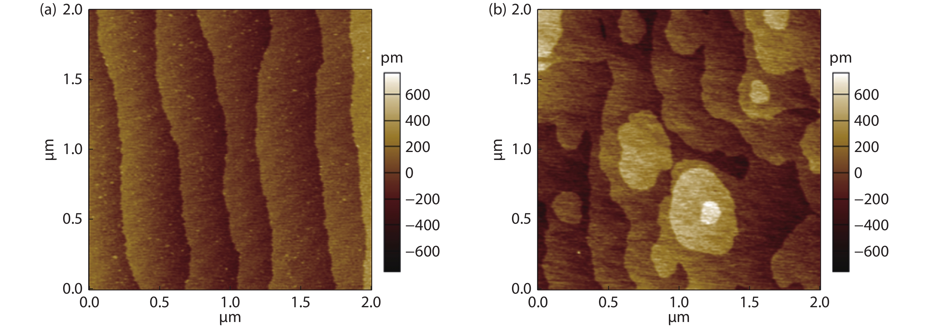
The structures were fully grown using a low-pressure (100 mbar) MOCVD with a close-coupled showerhead reactor. Group III precursors are trimethylindium (TMIn), trimethylgallium (TMGa), and trimethylaluminum (TMAl). Group V precursors are arsine and phosphine. The n-type dopant is SiH4 (0.02% in H2). Typical growth parameters are in the ranges: substrate temperatures 600–700 °C; growth rates for QCL active components (In0.53Ga0.47As and In0.52Al0.48As) 0.1–0.5 nm/s; growth rates for waveguide and cladding layers (n-type doped InP) 0.3–0.8 nm/s; V/III ratios 15–200; growth interrupts at the interfaces of InGaAs-to-InAlAs and InAlAs-to-InGaAs 0–5 s. The QCL active region consists of ~500–1000 InGaAs wells and InAlAs barrier layers, with thicknesses ranging between 0.5 to 6 nm, and the precisions of thickness and alloy composition should be achieved as best as we can. To put this in perspective, we first realized lattice matched 1 μm-thick In0.53Ga0.47As and In0.52Al0.48As by varying the growth parameters. The optimal ranges were determined by the background doping and electron mobility obtained from Hall measurement and the surface morphology obtained from atomic force microscopy (AFM).Fig. 1 shows the surface images of lattice-matched In0.53Ga0.47As (left) and In0.52Al0.48As (right) layers measured by AFM. Step-flow mode can be observed, indicating good surface morphology. The morphology of InAlAs shows moderate degradation, which is reasonable due to the low migration rate of Al atoms. Precise control over the layer thicknesses and compositions was ensured using process calibration with the combination of optical in-situ and ex-situ techniques, such as scanning electron microscopy (SEM) and high resolution X-ray diffraction (XRD). Then the QCL structure can be grown under specify growth conditions.
![]()
Figure 1.AFM images (2 × 2
Considering the relatively large allowance for structure fluctuations, single phonon resonance-continuum depopulation QCL structure was adopted[
The QCL structure similar to Ref. [11] was fully grown on n-doped InP substrate (S, 2 × 1018 cm−3). The layer thicknesses in nanometers, starting from the first injection barrier, are as follows:
Fig. 2(a) compares the measured and simulated high-resolution XRD results. Experimental result is almost fully in line with the simulated one. Fig. 2(b) shows the enlarged view of satellite diffraction peaks with full width at half maximum (FWHM) labelled, which are given by fitting the peaks with a Gaussian distribution. Multiple high-order satellite peaks can be clearly observed with extremely sharp and narrow FWHM of about 30 arcsec. In order to characterize interfaces smoothness, it is crucial to have a reliable means of determining the IFR in the grown structures. A rapid and efficient technique is the high-resolution XRD[
![]()
Figure 2.(a) High-resolution XRD of experimental (blue, upper curve) and simulated (red, lower curve) results of lattice-matched QCL structures. (b) Partially enlarged view of satellite diffraction peaks. The full-width at half-maximum (FWHM) of satellite diffraction peaks are labelled in arcsec.
3. Device performance
The fabrication process of QCLs is as follows. The wafer was processed into a buried hetero-structure (BH) configuration with a ridge width of 10 μm. Firstly, the wafer was patterned into stripes along with [110] direction by using a 300 nm-thick SiO2 mask and wet-etched through the active region into a double-channel geometry. The etchant is 1 : 1 : 10 HBr : HNO3 : H2O which is non-selective and isotropic. The etching depth was controlled step by step down to the bottom of the active region with an etching profile similar to a trapezoid geometry. After etching and rinsing, Fe-doped semi-insulating InP was selective-area regrown by MOCVD to planarize the channels. In order to guarantee the quality of InP in channels, the etching profile should be well controlled. Considering wet etching is soft, different profile can be easily achieved. Wet etching was chosen to form specific channels profile. Then SiO2 mask was removed, and a new 300 nm-thick SiO2 layer was deposited by plasma-enhanced chemical vapor deposition as an electrical isolation layer. The current injection windows were opened on the top of the ridge by lithography and HF etching. Besides, top contact was made, including a Ti/Au layer by e-beam evaporation and a 5 μm-thick Au layer by electroplating. After the wafer was thinned down to 120 μm and polished, an AuGeNi/Au layer was evaporated as the bottom contact. Finally, the processed wafer was cleaved into 4 mm bars, and a high-reflectivity coating consisting of Al2O3/Ti/Au/Ti/Al2O3 (200/10/100/10/120 nm) was applied on the back facet with the front facet left uncoated. For packaging, the chips were soldered epi-down on diamond submounts to improve heat removal efficiency. Then the submounts with chips were mounted on the copper heat sinks with indium solder followed by wire bonding.
Fig. 3(a) shows CW power and applied voltage versus current (PIV) curve at different temperatures. The CW optical power was measured by fixing a laser on the water-cooling platform with a chip facet close to a calibrated thermopile detector. The temperature was monitored by a thermistor and controlled by a thermoelectric cooler (TEC). A total amount of 1.04 W CW output power was obtained at 288 K, with a threshold current density of 1.18 kA/cm2. Fig. 3(b) shows the calculated WPE versus injection current at different temperatures. The maximum WPE is 7.1% at 288 K, which is higher than all previously published results obtained from MOCVD-grown LWIR QCLs. In addition, the threshold current density presented here is among the lowest (1.6 kA/cm2 in Ref. [20], and 2.5 kA/cm2 in Ref. [21]) when compared with other high-power (watt-level) LWIR QCLs.
![]()
Figure 3.(a) Power–current–voltage relations of 10
Besides relatively high efficiency and low threshold current density, a remarkable feature is that QCLs work up to 408 K in CW mode with the output power of 160 mW and the WPE of 1%. This distinctive feature gives the direct evidence that the QCLs are robust. CW operation in high temperature is difficult to achieve which limited by the natural cascade characteristic of QCLs. A dedicated effort has been put from the perspective of the active region, waveguide optimization, device process, and thermal management[
Fig. 4 shows temperature-dependent threshold current density Jth and slope efficiency η in pulse mode. According to the empirical formulas:
![]()
Figure 4.Threshold current density and slope efficiency at different temperatures in pulse conditions at 1
whereT is the heat sink temperature, T0 and T1 are the characteristic temperature coefficient of the pulsed threshold-current density and slope efficiency. The fitting parameters are T0 = 178 K and T1 = 365 K. Besides the relatively low threshold current density, the T0 of the device is comparable with the best value from the MBE-grown QCLs with AlN submounts[
Combining with the above characterization of material properties, it is credible to ascribe the high performances of our QCLs to the reduced IFR. The IFR can be approximated by parameterizing the random roughness profile of the interface, i.e., the average root-mean-square height ∆ and the characteristic lateral dimension Λ of the roughness. The IFR scattering rate of a QCL is given by[
where m* is the conduction band electron effective mass,
Fig. 5(a) shows the device lasing spectrum at room temperature. Emission spectrum centering at 1175 cm–1 (8.5 μm) was obtained by Fourier transformed infrared spectrometer (FTIR) with a resolution of 0.25 cm–1 in rapid scan mode. The transverse mode is another characteristic affecting the actual application of QCLs. Fig. 5(b) shows the beam image in pulse mode operation. The fundamental transverse mode could be clearly observed by placing a pyroelectric camera 20 cm away from the collimated chip, demonstrating this TM00 beam is suitable for practical applications.
![]()
Figure 5.(a) Emission spectrum at current slightly above threshold. (b) Beam picture in pulse mode at room temperature.
4. Conclusion
In conclusion, high-performance CW operation QCL grown by MOCVD is demonstrated. High-quality interface quantum cascade structures can be realized by carefully controlling and optimizing growth conditions. The 4 mm-long, HR-coated QCL device exhibits 1.04 W CW output at 288 K at
Acknowledgements
The authors would thank Ping Liang and Ying Hu for their help with device fabrication. This work was supported by the National Key Research and Development Program of China (Grant No. 2020YFB0408401), in part by the National Natural Science Foundation of China (Grant Nos. 61991430, 61774146, 61790583, 61734006, 61835011, 61674144, 61774150, 61805168), in part by Beijing Municipal Science & Technology Commission (Grant No. Z201100004020006), and in part by the Key Projects of the Chinese Academy of Sciences (Grant Nos. 2018147, YJKYYQ20190002, QYZDJ-SSW-JSC027, XDB43000000, ZDKYYQ20200006).
References
[1] J Faist, F Capasso, D Sivco et al. Quantum cascade laser. Science, 264, 553(1994).
[2] A Hugi, G Villares, S Blaser et al. Mid-infrared frequency comb based on a quantum cascade laser. Nature, 492, 229(2012).
[3] J Zhang, L Wang, W Zhang et al. Holographic fabricated continuous wave operation of distributed feedback quantum cascade lasers at λ ≈ 8.5
[4] J Faist, M Beck, T Allen et al. Quantum-cascade lasers based on a bound-to-continuum transition. Appl Phys Lett, 78, 147(2001).
[5] M Beck, D Hofstetter, T Aellen et al. Continuous wave operation of a mid-infrared semiconductor laser at room temperature. Science, 295, 301(2002).
[6] D Botez, J D Kirch, C Boyle et al. High-efficiency, high-power mid-infrared quantum cascade lasers. Opt Mater Express, 8, 1378(2018).
[7] C A Wang, B Schwarz, D F Siriani et al. MOVPE growth of LWIR AlInAs/GaInAs/InP quantum cascade lasers: Impact of growth and material quality on laser performance. IEEE J Sel Top Quantum Electron, 23, 1(2017).
[8] X Feng, C Caneau, H P Leblanc et al. Watt-level room temperature continuous-wave operation of quantum cascade lasers with λ >10
[9] B Schwarz, C A Wang, L Missaggia et al. Watt-level continuous-wave emission from a bifunctional quantum cascade laser/detector. ACS Photonics, 4, 1225(2017).
[10] W Zhou, Q Y Lu, D H Wu et al. High-power, continuous-wave, phase-locked quantum cascade laser arrays emitting at 8 microm. Opt Express, 27, 15776(2019).
[11] C A Wang, B Schwarz, D F Siriani et al. Sensitivity of heterointerfaces on emission wavelength of quantum cascade lasers. J Cryst Growth, 464, 215(2017).
[12] A Lyakh, R Maulini, A Tsekoun et al. 3 W continuous-wave room temperature single-facet emission from quantum cascade lasers based on nonresonant extraction design approach. Appl Phys Lett, 95, 141113(2009).
[13] J B Khurgin, Y Dikmelik, P Q Liu et al. Role of interface roughness in the transport and lasing characteristics of quantum-cascade lasers. Appl Phys Lett, 94, 091101(2009).
[14] K Fujita, S Furuta, A Sugiyama et al. High-performance λ ~8.6
[15] P Figueiredo, M Suttinger, R Go et al. Progress in high-power continuous-wave quantum cascade lasers. Appl Opt, 56, H15(2017).
[16] T Yu, S Liu, J Zhang et al. InAs-based interband cascade lasers at 4.0
[17] P F Fewster. Interface roughness and period variations in MQW structures determined by X-ray diffraction. J Appl Cryst, 21, 524(1988).
[18] P F Fewster. X-ray diffraction from low-dimensional structures. Semicond Sci Technol, 8, 1915(1993).
[19] D Savage, J Kleiner, N Schimke et al. Determination of roughness correlations in multilayer films for x-ray mirrors. J Appl Phys, 69, 1411(1991).
[20] D Botez, C C Chang, L J Mawst. Temperature sensitivity of the electro-optical characteristics for mid-infrared (λ = 3–16
[21] A Lyakh, R Maulini, A Tsekoun et al. Multiwatt long wavelength quantum cascade lasers based on high strain composition with 70% injection efficiency. Opt Express, 20, 24272(2012).
[22] P Yang, J Zhang, Z Gu et al. Coupled-ridge waveguide quantum cascade laser array lasing at λ ~ 5 µm. J Semicond, 42, 092901(2021).
[23] A Wittmann, Y Bonetti, M Fischer et al. Distributed-feedback quantum-cascade lasers at 9
[24] Y Chiu, Y Dikmelik, P Q Liu et al. Importance of interface roughness induced intersubband scattering in mid-infrared quantum cascade lasers. Appl Phys Lett, 101, 171117(2012).
[25] G Xu, A Li. Interface phonons in the active region of a quantum cascade laser. Phys Rev B, 71, 235304(2005).
[26] C Boyle, K M Oresick, J D Kirch et al. Carrier leakage via interface-roughness scattering bridges gap between theoretical and experimental internal efficiencies of quantum cascade lasers. Appl Phys Lett, 117, 051101(2020).
[27] M P Semtsiv, Y Flores, M Chashnikova et al. Low-threshold intersubband laser based on interface-scattering-rate engineering. Appl Phys Lett, 100, 163502(2012).


Set citation alerts for the article
Please enter your email address

© Copyright 2018-2021 | Chinese Laser Press. All Rights Reserved 沪ICP备15018463号-20