Pei Yuan, Lixiu Zhang, Menghua Zhu, Liming Ding. Perovskite films for X-ray detection[J]. Journal of Semiconductors, 2022, 43(7): 070202
Search by keywords or author
- Journal of Semiconductors
- Vol. 43, Issue 7, 070202 (2022)
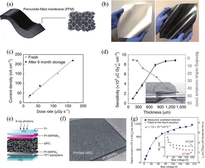
![(Color online) (a) Perovskite-filled membrane (PFM). (b) A 400 cm2 nylon membrane without (left) and with (right) perovskites. (c) Current density for the PFM device changes with the dose rate. (d) Dependence of the sensitivity and flexibility of PFM devices on device thicknesses. Inset: the bending of a PFM device. The error bars were obtained from three devices. Reproduced with permission[21], Copyright 2020, Springer Nature. (e) Illustration for an all-solution-processed X-ray detector. (f) Printed MPC on PI-MAPbI3. (g) Signal current and sensitivity change with bias voltage. Reproduced with permission[22], Copyright 2017, Springer Nature.](/richHtml/jos/2022/43/7/070202/jos_43_7_070202_f1.jpg)
Fig. 1. (Color online) (a) Perovskite-filled membrane (PFM). (b) A 400 cm2 nylon membrane without (left) and with (right) perovskites. (c) Current density for the PFM device changes with the dose rate. (d) Dependence of the sensitivity and flexibility of PFM devices on device thicknesses. Inset: the bending of a PFM device. The error bars were obtained from three devices. Reproduced with permission[21 ], Copyright 2020, Springer Nature. (e) Illustration for an all-solution-processed X-ray detector. (f) Printed MPC on PI-MAPbI3. (g) Signal current and sensitivity change with bias voltage. Reproduced with permission[22 ], Copyright 2017, Springer Nature.
![(Color online) (a) The lamination technique. (b) Heterojunction perovskite film. (c) Response of single-composition and heterojunction perovskite detectors. Reproduced with permission[27], Copyright 2021, AAAS. (d) Wet film fabrication by spin-coating or blade-coating. (e) The ALS method. (f) The nucleation and growth process in (d). (g) Nucleation and growth process in ALS method. Reproduced with permission[30], Copyright 2021, Elsevier.](/richHtml/jos/2022/43/7/070202/jos_43_7_070202_f2.jpg)
Fig. 2. (Color online) (a) The lamination technique. (b) Heterojunction perovskite film. (c) Response of single-composition and heterojunction perovskite detectors. Reproduced with permission[27 ], Copyright 2021, AAAS. (d) Wet film fabrication by spin-coating or blade-coating. (e) The ALS method. (f) The nucleation and growth process in (d). (g) Nucleation and growth process in ALS method. Reproduced with permission[30 ], Copyright 2021, Elsevier.

Set citation alerts for the article
Please enter your email address


