Author Affiliations
1State Key Laboratory of Solidification Processing, Key Laboratory of Radiation Detection Materials and Devices, School of Materials Science and Engineering, Northwestern Polytechnical University, Xi’an 710072, China2Center for Excellence in Nanoscience (CAS), Key Laboratory of Nanosystem and Hierarchical Fabrication (CAS), National Center for Nanoscience and Technology, Beijing 100190, Chinashow less
X-ray detection is widely used in research[1-3], product inspection[4], nuclear station, and medical imaging. Si[5], α-Se[6], PbI2[7], and CdZnTe[8] are conventional semiconductors, and some problems limit their applications. For instance, Si and α-Se have low stopping power for X-ray[8], which hinders their application in high-energy range over 50 keV. Moreover, the complicated preparation, high operating voltage, and high fabrication cost of these materials are the negative issues.
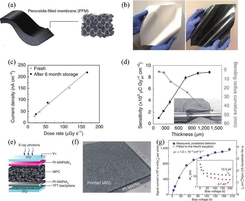
In comparison to brittle single-crystal films, polycrystalline films can be curved to fit non-flat substrates, thus showing potential for flexible X-ray detectors[18, 19]. Some high-quality flexible perovskite films were prepared, presenting high performance. Liu et al.[20] reported a flexible and printable X-ray detector based on colloidal CsPbBr3 QDs. To enhance the sensitivity, they effectively reduced the surface defects and tuned crystallinity via chemical engineering. This detector can sense a very low X-ray dose rate (~17.2 µGy s–1) with a high sensitivity of 1450 µC Gy–1 cm–2 at 0.1 V bias. Meanwhile, the vignetting issues can be effectively alleviated, leading to reduced misdiagnosis. 400 cm2 MAPb(I0.9Cl0.1)3-filled nylon membranes were used to make X-ray detectors[21]. The devices exhibited a high sensitivity of ~8696 μC Gy–1 cm–2 and could be bent at 2 mm radius without performance loss (Figs. 1(a)–1(d)).
Perovskite materials are promising candidates for X-ray detection due to facile synthesis[9-14] and large mobility-lifetime (μτ) products for highly sensitive detection. The μτ product of MAPbBr3 single crystal reaches 1.2 × 10⁻² cm2 V–1[12], which is comparable to the μτ value of CdZnTe[3]. Perovskite-based X-ray detectors also exhibited a record X-ray sensitivity[15] of ~710 000 μC Gy–1 cm–2 and an ultralow detection limit[16] of 0.62 nGy s–1. Tang et al. developed a hot-pressing method to grow quasi-monocrystalline CsPbBr3 films, which exhibits a superior sensitivity of 55 684 μC Gy–1 cm–2 and a low detection limit of 215 nGy s–1[17]. To date, halide perovskites in various forms like polycrystalline films, single crystals, and nanocrystals have been used in X-ray detectors. Especially, polycrystalline films prepared by hot-pressing, coating or printing have attracted great interests due to their superior flexibility, lightweight and facile synthesis.
![(Color online) (a) Perovskite-filled membrane (PFM). (b) A 400 cm2 nylon membrane without (left) and with (right) perovskites. (c) Current density for the PFM device changes with the dose rate. (d) Dependence of the sensitivity and flexibility of PFM devices on device thicknesses. Inset: the bending of a PFM device. The error bars were obtained from three devices. Reproduced with permission[21], Copyright 2020, Springer Nature. (e) Illustration for an all-solution-processed X-ray detector. (f) Printed MPC on PI-MAPbI3. (g) Signal current and sensitivity change with bias voltage. Reproduced with permission[22], Copyright 2017, Springer Nature.](/Images/icon/loading.gif)
Figure 1.(Color online) (a) Perovskite-filled membrane (PFM). (b) A 400 cm2 nylon membrane without (left) and with (right) perovskites. (c) Current density for the PFM device changes with the dose rate. (d) Dependence of the sensitivity and flexibility of PFM devices on device thicknesses. Inset: the bending of a PFM device. The error bars were obtained from three devices. Reproduced with permission[21], Copyright 2020, Springer Nature. (e) Illustration for an all-solution-processed X-ray detector. (f) Printed MPC on PI-MAPbI3. (g) Signal current and sensitivity change with bias voltage. Reproduced with permission[22], Copyright 2017, Springer Nature.
Generally, perovskite films should have a thickness of hundreds micrometers for sufficient X-ray absorption[28]. However, it is very difficult to make such films by spin-coating or blade-coating methods. First, it is difficult to deposit a very thick wet film due to the limitations of surface tension and viscosity[29]. Second, even though a thick wet film could be made, it is still difficult to obtain perovskite films with high crystallinity and low defect density (Figs. 2(d) and 2(f)). To solve this issue, Wei et al.[30] developed an aerosol–liquid–solid (ALS) method to make perovskite films on TFT substrates by spray coating. This method solved the problem of uncontrolled crystallization of perovskites (Figs. 2(e) and 2(g)). The detectors demonstrated a high sensitivity (~1.48 × 10⁵μC Gy–1 cm–2), a low detection limit (280 nGy s–1), and they could also realize high-resolution imaging.
In summary, high-quality perovskite films featuring large area, sufficient thickness, flexibility and high sensitivity are prerequisites for high-performance X-ray detectors. Perovskite X-ray detectors may find applications in security inspection, medical imaging, and nondestructive checking in the future.
The perovskite films should give low dark current to ensure high X-ray sensitivity. The patients under a high level of radiation exposure may face cancer risk[24]. To capture clear X-ray images under a low dose of X-ray is desired[25]. The detection limit is the minimum signal which can be reliably identified by X-ray detectors and is defined as the equivalent dose rate of a signal 3 times greater than the noise. A low detection limit results from high current signal with low noise current dominated by dark current, which can reduce the imaging capability of detectors under weak X-ray. Most polycrystalline perovskite detectors[17, 26] have large dark current densities of 50–500 nA cm–2 under an electrical field of 0.05 V μm–1 due to the defective structures as compared to single crystals. To solve this problem, great efforts have been devoted to improve the quality of perovskite films. Zhou et al.[27] reported a heterojunction structure formed by laminating membranes filled with perovskites with different bandgaps. The membranes reduced dark current density of the devices by over 200 times without compromising their sensitivity. They captured clear X-ray images at a low dose rate of 32.2 nGy s–1 (Figs. 2(a)–2(c)). Tang et al.[23] also proposed a new strategy to suppress ion migration by inserting 2D Ruddlesden-Popper layer into 3D perovskite film. The quasi-2D perovskite X-ray detector offered a sensitivity of 10 860 µC Gy–1 cm–2 with a stable dark current.
Figure 2.(Color online) (a) The lamination technique. (b) Heterojunction perovskite film. (c) Response of single-composition and heterojunction perovskite detectors. Reproduced with permission[27], Copyright 2021, AAAS. (d) Wet film fabrication by spin-coating or blade-coating. (e) The ALS method. (f) The nucleation and growth process in (d). (g) Nucleation and growth process in ALS method. Reproduced with permission[30], Copyright 2021, Elsevier.
For polycrystalline films, besides flexibility, the facile preparation of large-area and thick films by solution processing is another advantage over single crystal films. Blade coating is one of the common methods. Kim et al.[22] made a thick polycrystalline MAPbI3 film by this method, and it had excellent optoelectronic properties, which are comparable to single crystal films. The device had a thickness of 830 μm and an active area of ~100 cm2 (Figs. 1(e)–1(g)). In order to minimize dark current drift, the polycrystalline films should have high crystallinity and large grain to reduce grain boundaries. He et al.[23] made a quasi-2D perovskite film with low defects and suppressed ion migration. The average grain size was 31.88 µm. Such large grain size resulted from colloidal particles aggregating in the slurry with PEA+, which can decrease nucleation sites. The resulted µτ value was 2.6 × 10⁻⁵ cm2 V–1 and the minimum current drift was 1.5 × 10⁻² pA cm–1 s–1 V–1.
Acknowledgements
M. Zhu thanks the National Natural Science Foundation of China (62104194) for financial support. L. Ding thanks the National Key Research and Development Program of China (2017YFA0206600), the National Natural Science Foundation of China (51922032 and 21961160720), and the open research fund of Songshan Lake Materials Laboratory (2021SLABFK02) for financial support.
References
[1] Y Zhou, J Chen, O M Bakr et al. Metal halide perovskites for X-ray imaging scintillators and detectors. ACS Energy Lett, 6, 739(2021).
[2] H Wu, Y Ge, G Niu et al. Metal halide perovskites for X-ray detection and imaging. Matter, 4, 144(2021).
[3] H Wei, J Huang. Halide lead perovskites for ionizing radiation detection. Nat Commun, 10, 1066(2019).
[4] A Olivo, D Chana, R Speller. A preliminary investigation of the potential of phase contrast X-ray imaging in the field of homeland security. J Phys D, 41, 225503(2008).
[5] M Guerra, M Manso, S Longelin et al. Performance of three different Si X-ray detectors for portable XRF spectrometers in cultural heritage applications. J Instrum, 7, C10004(2012).
[6] S Kasap. X-ray sensitivity of photoconductors: application to stabilized α-Se. J Phys D, 33, 2853(2000).
[7] R Street, S Ready, K Van Schuylenbergh et al. Comparison of PbI2 and HgI2 for direct detection active matrix X-ray image sensors. J Appl Phys, 91, 3345(2002).
[8] S Del Sordo, L Abbene, E Caroli et al. Progress in the development of CdTe and CdZnTe semiconductor radiation detectors for astrophysical and medical applications. Sensors, 9, 3491(2009).
[9] Y Su, W Ma, Y M Yang. Perovskite semiconductors for direct X-ray detection and imaging. J Semicond, 41, 051204(2020).
[10] S Yakunin, D N Dirin, Y Shynkarenko et al. Detection of gamma photons using solution-grown single crystals of hybrid lead halide perovskites. Nat Photonics, 10, 585(2016).
[11] J Huang, Y Yuan, Y Shao et al. Understanding the physical properties of hybrid perovskites for photovoltaic applications. Nat Rev Mater, 2, 17042(2017).
[12] H Wei, Y Fang, P Mulligan et al. Sensitive X-ray detectors made of methylammonium lead tribromide perovskite single crystals. Nat Photonics, 10, 333(2016).
[13] F Zhou, Z Li, W Lan et al. Halide perovskite, a potential scintillator for X-ray detection. Small Methods, 4, 2000506(2020).
[14] C Li, Y Ma, Y Xiao et al. Advances in perovskite photodetectors. InfoMat, 2, 1247(2020).
[15] Y Song, L Li, W Bi et al. Atomistic surface passivation of CH3NH3PbI3 perovskite single crystals for highly sensitive coplanar-structure X-ray detectors. Research, 2020, 5958243(2020).
[16] X Zheng, W Zhao, P Wang et al. Ultrasensitive and stable X-ray detection using zero-dimensional lead-free perovskites. J Energy Chem, 49, 299(2020).
[17] W Pan, B Yang, G Niu et al. Hot-pressed CsPbBr3 quasi-monocrystalline film for sensitive direct X-ray detection. Adv Mater, 31, 1904405(2019).
[18] H Thirimanne, K Jayawardena, A Parnell et al. High sensitivity organic inorganic hybrid X-ray detectors with direct transduction and broadband response. Nat Commun, 9, 2926(2018).
[19] S Demchyshyn, M Verdi, L Basirico et al. Designing ultraflexible perovskite X-ray detectors through interface engineering. Adv Sci, 7, 2002586(2020).
[20] J Liu, B Shabbir, C Wang et al. Flexible, printable soft-X-ray detectors based on all-inorganic perovskite quantum dots. Adv Mater, 31, 1901644(2019).
[21] J Zhao, L Zhao, Y Deng et al. Perovskite-filled membranes for flexible and large-area direct-conversion X-ray detector arrays. Nat Photonics, 14, 612(2020).
[22] Y C Kim, K H Kim, D Y Son et al. Printable organometallic perovskite enables large-area, low-dose X-ray imaging. Nature, 550, 87(2017).
[23] X He, M Xia, H Wu et al. Quasi-2D perovskite thick film for X-ray detection with low detection limit. Adv Funct Mater, 32, 2109458(2021).
[24] A Datta, Z Zhong, S Motakef. A new generation of direct X-ray detectors for medical and synchrotron imaging applications. Sci Rep, 10, 20097(2020).
[25] D J Brenner, C D Elliston, E J Hall et al. Estimated risks of radiation-induced fatal cancer from pediatric CT. Am J Roentgenol, 176, 289(2001).
[26] B Yang, W Pan, H Wu et al. Heteroepitaxial passivation of Cs2AgBiBr6 wafers with suppressed ionic migration for X-ray imaging. Nat Commun, 10, 1989(2019).
[27] Y Zhou, L Zhao, Z Ni et al. Heterojunction structures for reduced noise in large-area and sensitive perovskite X-ray detectors. Sci Adv, 7, eabg6716(2021).
[28] H S Gill, B Elshahat, A Kokil et al. Flexible perovskite based X-ray detectors for dose monitoring in medical imaging applications. Phys Med, 5, 20(2018).
[29] S Chen, X Xiao, B Chen et al. Crystallization in one-step solution deposition of perovskite films: Upward or downward. Sci Adv, 7, eabb2412(2021).
[30] W Qian, X Xu, J Wang et al. An aerosol-liquid-solid process for the general synthesis of halide perovskite thick films for direct-conversion X-ray detectors. Matter, 4, 942(2021).