
Qiang Liu, Qian Wang, Hao Liu, Chenxi Fei, Shiyan Li, Runhua Huang, Song Bai. Low on-resistance 1.2 kV 4H-SiC power MOSFET with Ron, sp of 3.4 mΩ·cm2[J]. Journal of Semiconductors, 2020, 41(6): 062801
- Journal of Semiconductors
- Vol. 41, Issue 6, 062801 (2020)
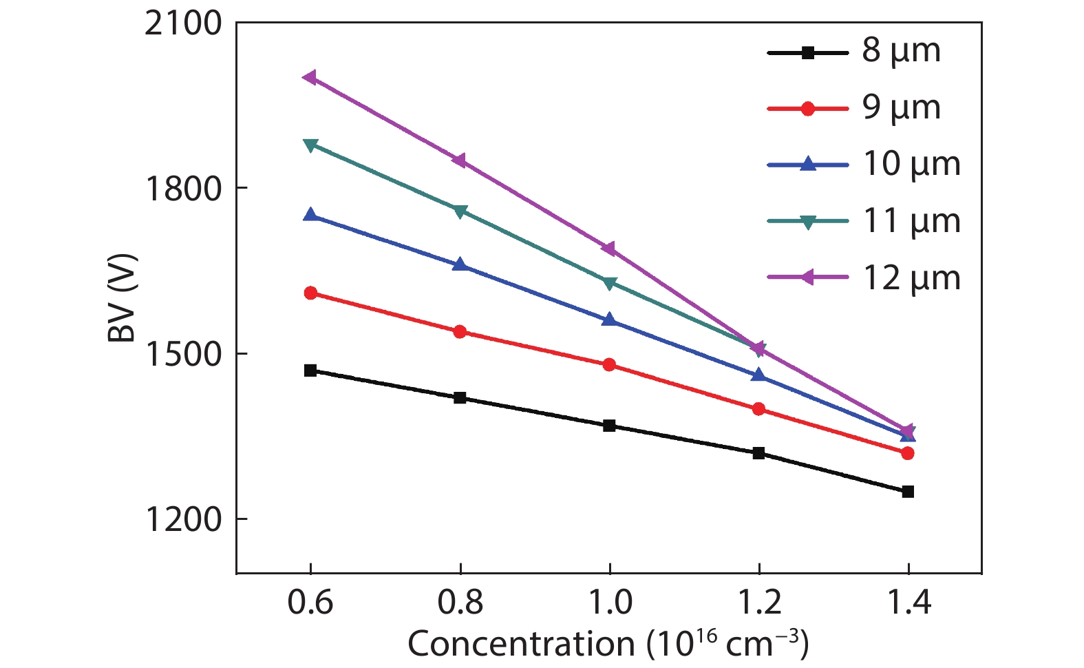
Fig. 1. (Color online) Theoretical breakdown voltages of epi-layers with various thickness and doping concentration.
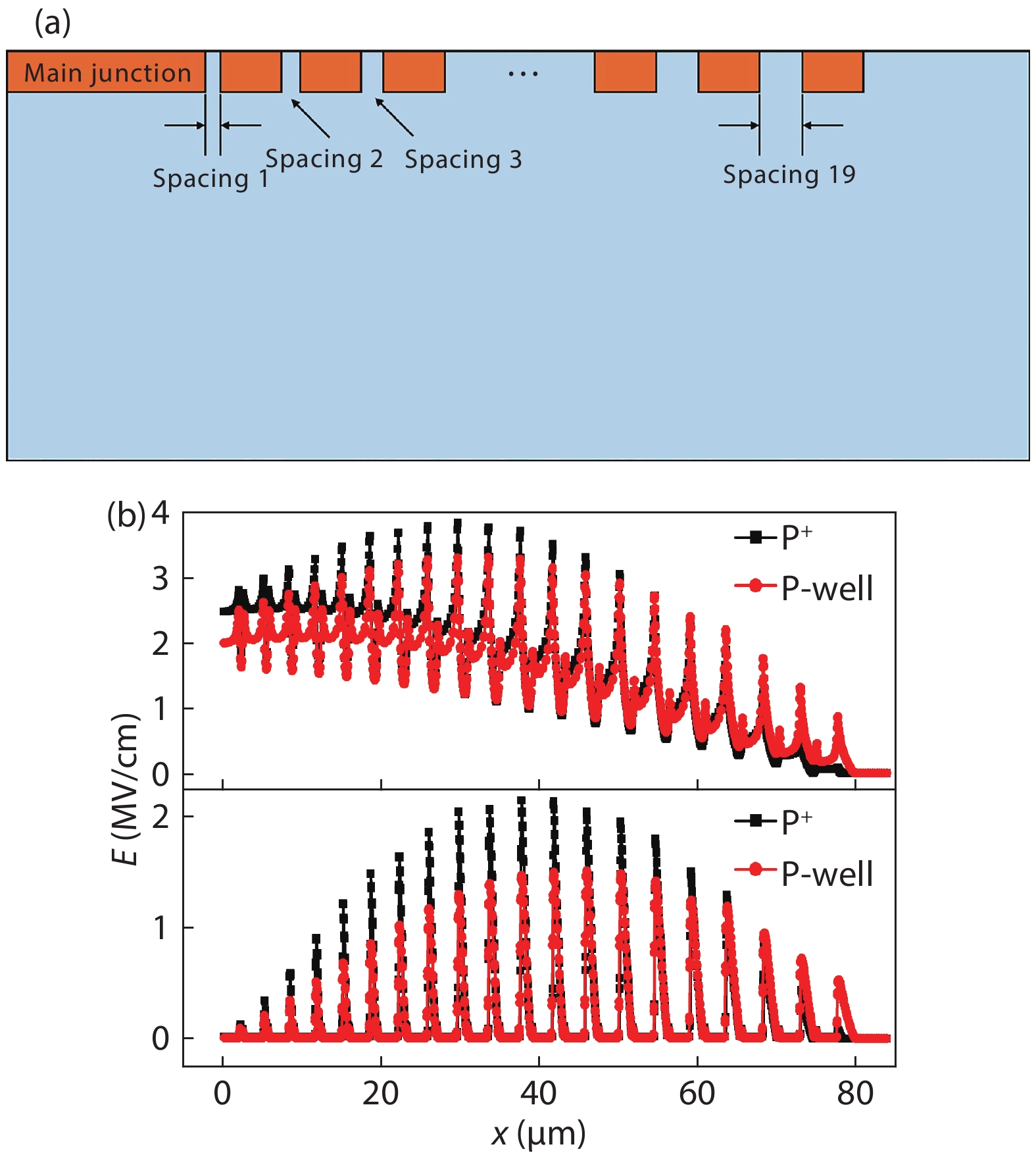
Fig. 2. (Color online) (a) Modeled FGR type edge termination structure. (b) E-field strength profiles comparison between P-well doped and P+ doped FGR type edge termination. Both data are extracted under breakdown statuses of the two terminations, respectively. Upper one corresponds to E-field at the depth of p–n junction and bottom one corresponds to E-field near the surface of the edge termination.
Fig. 3. Breakdown voltages of FGR with different spacing arrays.
Fig. 4. (Color online) (a) Specific on-resistance with and without additional JFET doping. (b) Electric field strength in gate oxide and specific on-resistance dependence on JFET width.
Fig. 5. (Color online) Doping regions of designed SiC MOSFET including P-well, N+, P+, and JFET regions.
Fig. 6. (Color online) Photo of fabricated 1.2 kV / 15 mΩ devices.
Fig. 7. (Color online) Breakdown voltages of PiN diodes with different FGR spacing arrays.
Fig. 8. (Color online) Current–voltage curves of various gate voltages.
Fig. 9. (Color online) Drain–source leakage current at V GS = 0 V. The dashed red line represents V DS = 1.5 kV.


Set citation alerts for the article
Please enter your email address

© Copyright 2018-2021 | Chinese Laser Press. All Rights Reserved 沪ICP备15018463号-20