
Qiang Liu, Qian Wang, Hao Liu, Chenxi Fei, Shiyan Li, Runhua Huang, Song Bai. Low on-resistance 1.2 kV 4H-SiC power MOSFET with Ron, sp of 3.4 mΩ·cm2[J]. Journal of Semiconductors, 2020, 41(6): 062801
- Journal of Semiconductors
- Vol. 41, Issue 6, 062801 (2020)
Abstract
1. Introduction
SiC MOSFETs have achieved great improvements, both in device design and material fabrication technology[
In our previous work, we (i.e. Huang) developed a 1200 V /40 mΩ MOSFET[
2. Design and simulation
Our simulated models and simulation results will be discussed in this section, including epi-layer parameters, floating guard ring (FGR) type edge termination, cell pitch geometry and JFET region.
2.1. Determination of epi-layer parameters
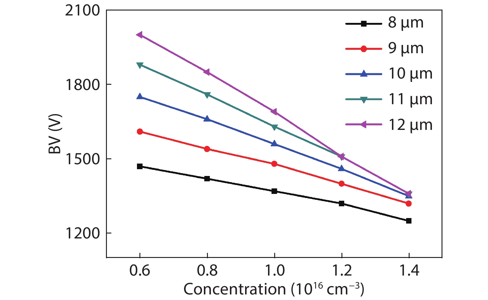
The target voltage rating is mainly supported by the thickness and doping concentration of the epi-layer, which shall be taken into consideration at the beginning of device design. A planar junction with the same doping depth as the P-well is modeled and simulated by SILVACO ATLAS TCAD. Fig. 1 shows the theoretical breakdown voltages (BV) of modeled planar junction structures. The thickness of epi-layer varies from 8 to 12 μm, and the n-type doping concentration varies from 6 × 10¹⁵ to 1.4 × 1016 cm−3. The BV increases while adding the thickness and decreasing the doping concentration of epi-layer. Because we aim to design a device with a voltage rating of 1.2 kV, the preferred BV should not be less than 1.5 kV. Following the simulation results, we choose a thickness of 10 μm and n-type doping concentration of 1.1 × 1016 cm−3 as parameters of the device drift epi-layer, corresponding to a BV of 1510 V. Compared with former results from Huang, the optimization of epi-layer results in specific on-resistance decreasing by about 0.4 mΩ·cm2.
![]()
Figure 1.(Color online) Theoretical breakdown voltages of epi-layers with various thickness and doping concentration.
2.2. Design of float guard ring (FGR) type edge termination
FGR type edge termination is selected thanks to its convenient fabrication process. An FGR with doping profile same with P-well is simulated. Fig. 2(a) shows an edge termination containing 19 rings with 2.5 μm width and first ring spacing of 0.8 μm. The following spacing between nearby rings increases gradually to 2.4 μm. Compared with P+ doped FGR edge termination, the P-well doped FGR edge termination has a lower maximum electric field (E-field) strength at the depth of p–n junction under breakdown states, as can be seen in Fig. 2(b). P-well and P+ doping was modeled with a junction depth of about 0.8 and 0.6 μm, respectively. P-well doping has a retrograde profile and P+ doping has a box-type profile with maximal doping concentration over 1 × 1020 cm–3. The E-field strength near the semiconductor surface is lower for P-well doped termination compared with that of P+ doped termination, and also under each one’s breakdown status. The lower electric field strength near the semiconductor surface indicates a lower drain-source leakage current and a better stability. We furtherly simulate P-well doped FGR edge termination with various ring spacing arrays. The baseline FGR is labeled as ‘T’, while ‘T + 0.1’ refers to add 0.1 μm to all numbers in array ‘T’. ‘T + 0.2’, ‘T – 0.1’, and ‘T – 0.2’ are named in the same way. BVs of all FGR edge terminations are presented in Fig. 3. All BVs exceed 1.5 kV and ‘T – 0.1’ is desirable for the sake of stability during manufacture.
![]()
Figure 2.(Color online) (a) Modeled FGR type edge termination structure. (b) E-field strength profiles comparison between P-well doped and P+ doped FGR type edge termination. Both data are extracted under breakdown statuses of the two terminations, respectively. Upper one corresponds to E-field at the depth of p–n junction and bottom one corresponds to E-field near the surface of the edge termination.
![]()
Figure 3.Breakdown voltages of FGR with different spacing arrays.
2.3. Optimizing the cell pitch
To increase the current density, we constrict the width of P-well implanted region from 9 to 7 μm. The specific on-resistance is reduced by about 1.0 mΩ·cm2 while the JFET region is unchanged.
2.4. Optimization of electric field strength in gate oxide with additional n-type doping in JFET region
To design a planar type MOSFET, the JFET region is of great concern because of its considerable contribution to the total conducting resistance for MOSFETs with low-to-medium voltage ratings. To reduce the JFET region resistance, additional n-type doping is introduced. Fig. 4(a) shows the specific on-resistance of SiC MOSFET with and without n-type doping in JFET region. Without JFET doping (baseline), the on-resistance increases dramatically when constricting the JFET width. With additional n-type doping, the total doping concentration reaches 1 × 1017 cm−3 in the JFET region and the specific on-resistance obviously reduces. When choosing the JFET width, the electric field strength near the surface of JFET region is of great concern. When applying a proper VDS (turn off state) along the surface of JFET region, the electric field strength reaches its maximum at the middle point. The maximum value increases when increasing JFET width. Stronger field in JFET region results in a stronger field in gate oxide. We seek to keep the maximum value of E-field in gate oxide (Emax) below 4 MV/cm. Consequently, we simulate the electric field strength in gate oxide with JFET doping, the results can be seen in Fig. 4(b). A 2.6 μm JFET region is satisfied, at which the specific on-resistance is reduced by about 28% with JFET doping. If Emax is maintained under 3 MV/cm as usual (corresponds to 2.1 μm JFET), then the corresponding specific on-resistance will decrease by about 25% with JFET doping. For better reliability of the gate oxide, we choose to use 2.1 μm JFET in our design.
![]()
Figure 4.(Color online) (a) Specific on-resistance with and without additional JFET doping. (b) Electric field strength in gate oxide and specific on-resistance dependence on JFET width.
3. Fabrication
A 10 μm epi-layer with n-type doping concentration of 1.1 × 1016 cm−3 was grown on the ‘Si face’ of a heavily doped n-type 4H-SiC substrate, which was cut with an offset angle of 4 degrees. Doping regions are shown in Fig. 5 including P-well regions, N+ source regions, P+ regions, and JFET doping region.
![]()
Figure 5.(Color online) Doping regions of designed SiC MOSFET including P-well, N+, P+, and JFET regions.
P-well doping with retrograde profile was first achieved by several aluminum implantations. A heavily nitrogen doped region with box profile formed N+ source. The MOS channel was acquired by the self-alignment method, with a length of 0.7 μm. P+ regions were achieved by heavy dose aluminum doping. To reduce the resistance of the JFET region, additional low dose nitrogen doping was implemented. Doping of FGR type edge termination was realized at the same time with P-well process. After all of the doping processes, dopants were activated at 1870 K. Then, gate oxide layer (55 nm) was thermally grown at 1520 K in dry O2 ambient followed by an annealing process in NO ambient, also at 1520 K. Degenerated doped polysilicon layer (500 nm) was deposited and etched into the gate structure. Ohmic contact between nickel and N+ source/P+ region was formed by annealing at 1170 K in vacuum. Intermediate dielectric layer was deposited and via holes were opened soon after. Finally, thick metal layers were evaporated as electrodes at both sides of the wafer. The final wafer is shown in Fig. 6 and the target device is 5.2 × 5.5 mm2 with an active region area of 22.5 mm2.
![]()
Figure 6.(Color online) Photo of fabricated 1.2 kV / 15 mΩ devices.
A boron doped polysilicon gate was used instead of a phosphorus doped gate to obtain a higher gate threshold voltage.
4. Results and discussion
First, we verify the protection efficiency of FGR type edge termination with P-well doping. The breakdown voltages of PiN diodes are shown in Fig. 7. The designed edge termination structure has a breakdown voltage that is higher than 1550 V.
![]()
Figure 7.(Color online) Breakdown voltages of PiN diodes with different FGR spacing arrays.
Gate threshold voltage (VGS) is measured by applying VGS = VDS at which ID = 15 mA, which exhibits a typical value around 2.6 V, increasing by 0.5 V compared with phosphorus doped polysilicon gate. The pulsed current–voltage (I–V) curves under various gate voltages are shown in Fig. 8. This MOSFET conducts 50 A current at VDS = 0.75 V and VGS = 20 V, corresponding to an on-resistance of 15 mΩ and specific on-resistance of 3.4 mΩ·cm2.
![]()
Figure 8.(Color online) Current–voltage curves of various gate voltages.
The drain–source leakage current is measured by applying a step-by-step voltage to drain the electrode, while keeping source and gate electrodes shorted to ground. The leakage current is less than 1 μA at VDS = 1.4 kV, indicating a good turn off state, as shown in Fig. 9. The dashed-red line represents VDS = 1.5 kV. The breakdown voltage obviously exceeds 1.5 kV.
![]()
Figure 9.(Color online) Drain–source leakage current at
5. Conclusion
The design of our device is optimized by including epi-layer parameters, cell pitch size, doping concentration in JFET region and width of JFET region. Cell pitch size and JFET region optimizations both make significant efforts to the reduction of specific on-resistance. JFET region needs careful design for both doping concentration and width. These two parameters together count for the on-resistance and E-field in gate oxide (under turn-off state). By reducing cell pitch size, the specific on-resistance decreases by about 1 mΩ·cm2. By reducing JFET width and adding n-type doping in JFET region, the specific on-resistance decreases by about 1 mΩ·cm2 and the E-field in gate oxide is still in a safe range. Edge termination is also doped by P-well recipe and a lower maximum E-field is achieved under breakdown status. Finally, 1.2 kV / 15 mΩ SiC MOSFETs are realized with Ron, sp of 3.4 mΩ·cm2, breakdown voltage exceeding 1.5 kV and gate threshold voltage around 2.6 V.
Acknowledgements
This work was supported by the National Science and Technology Major Project (No. 2017YFB0102302).
References
[1] T Kimoto. Material science and device physics in SiC technology for high-voltage power devices. Jpn J Appl Phys, 54, 4(2015).
[2] D J Lichtenwalner, B Hull, V Pala et al. Performance and reliability of SiC power MOSFETs. MRS Adv, 1, 2(2016).
[3] A Castellazzi, A Fayyaz, G Romano et al. SiC power MOSFETs performance, robustness and technology maturity. Microelectron Reliab, 58, 58(2016).
[4] F Jiang, K Sheng, Q Guo et al. Comparative study of temperature-dependent characteristics for SiC MOSFETs. China International Forum on Solid State Lighting, 50(2016).
[5] W Zhou, Q Guo, X Wu et al. A 1200 V/100 A all-SiC power module for boost converter of EV/HEV’s motor driver application. China International Forum on Solid State Lighting, 38(2016).
[6]
[7]
[8]
[9]
[10] H Iwata, K M Itoh. Donor and acceptor concentration dependence of the electron Hall mobility and the Hall scattering factor in n-type 4H- and 6H-SiC. J Appl Phys, 89, 6228(2001).
[11] G Y Chung, C C Tin, J R Williams et al. Improved inversion channel mobility for 4H-SiC MOSFETs following high temperature anneals in nitric oxide. IEEE Electron Device Lett, 22, 176(2001).
[12] H A Moghadam, S Dimitrijev, J Han et al. Active defects in MOS devices on 4H-SiC: A critical review. Microelectron Reliab, 60, 60(2016).
[13] T Ohashi, Y Nakabayashi, T Shimizu et al. Investigation of nitridation and oxidation reactions at SiC/SiO2 interfaces in NO annealing and modeling of their quantitative impacts on mobility of SiC MOSFETs. Jpn J Appl Phys, 56, 10(2017).
[14] E Fujita, M Sometani, T Hatakeyama et al. Insight into enhanced field-effect mobility of 4H-SiC MOSFET with Ba incorporation studied by Hall effect measurements. AIP Adv, 8, 8(2018).
[15] P Fiorenza, L K Swanson, M Vivona et al. Characterization of SiO2/SiC interfaces annealed in N2O or POCl3. Materials Science Forum, 623(2014).
[16] H Rong, Y K Sharma, P A Mawby et al. Combined N2O and phosphorus passivations for the 4H-SiC/SiO2 interface with oxide grown at 1400 °C. Materials Science Forum, 344(2016).
[17] D J Lichtenwalner, V Pala, B Hull et al. High-mobility SiC MOSFETs with alkaline earth interface passivation. Materials Science Forum, 671(2016).
[18]


Set citation alerts for the article
Please enter your email address

© Copyright 2018-2021 | Chinese Laser Press. All Rights Reserved 沪ICP备15018463号-20