• Photonics Research
  • Vol. 10, Issue 7, A97 (2022)
Chandraman Patil1, Chaobo Dong1, Hao Wang1, Behrouz Movahhed Nouri1、2, Sergiy Krylyuk3, Huairuo Zhang3、4, Albert V. Davydov3, Hamed Dalir1、2, and Volker J. Sorger1、2、*
Author Affiliations
  • 1Department of Electrical and Computer Engineering, George Washington University, Washington, D.C. 20052, USA
  • 2Optelligence LLC, Upper Marlboro, Maryland 20772, USA
  • 3Materials Science and Engineering Division, National Institute of Standards and Technology, Gaithersburg, Maryland 20899, USA
  • 4Theiss Research, Inc., La Jolla, California 92037, USA
  • show less
    DOI: 10.1364/PRJ.441519 Cite this Article Set citation alerts
    Chandraman Patil, Chaobo Dong, Hao Wang, Behrouz Movahhed Nouri, Sergiy Krylyuk, Huairuo Zhang, Albert V. Davydov, Hamed Dalir, Volker J. Sorger. Self-driven highly responsive p-n junction InSe heterostructure near-infrared light detector[J]. Photonics Research, 2022, 10(7): A97 Copy Citation Text show less
    p-n heterojunction n-InSe/p-InSe photodetector. (a) Schematic representation of the n-InSe/p-InSe van der Waals p-n junction photodetector. (b) Optical micrograph image of the device (top view), where n-InSe was stacked on the top of the p-InSe flake, transferred on Au/Ti electrodes using the 2D printer technique. (c) Band diagram for p-InSe (red), n-InSe (green), and Au contact (yellow). (d) Raman spectra of the p-InSe, n-InSe, and the junction regions. All material-associated Raman peaks of p-InSe, n-InSe, and p-n InSe junction are observed to show peak positions and relative intensity associated with out-of-plane vibrational modes (A1g1 and A1g2) and in-plane vibrational modes (E2g1).
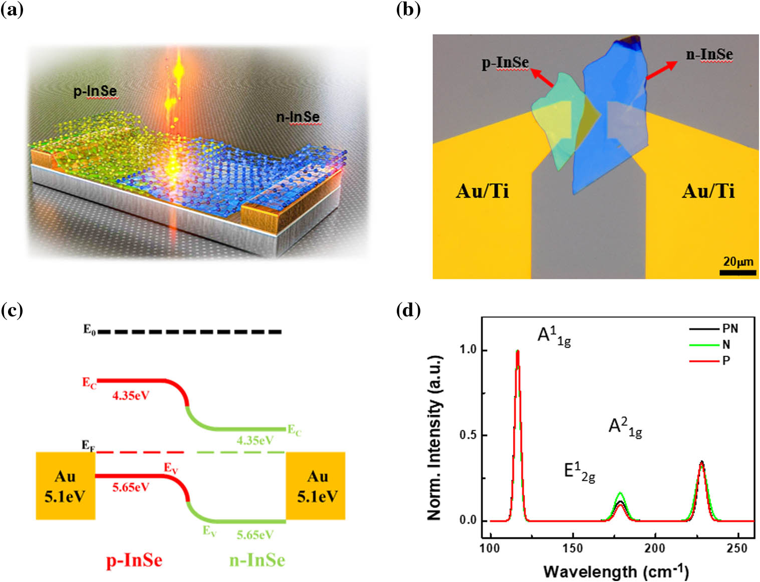
    Fig. 1. p-n heterojunction n-InSe/p-InSe photodetector. (a) Schematic representation of the n-InSe/p-InSe van der Waals p-n junction photodetector. (b) Optical micrograph image of the device (top view), where n-InSe was stacked on the top of the p-InSe flake, transferred on Au/Ti electrodes using the 2D printer technique. (c) Band diagram for p-InSe (red), n-InSe (green), and Au contact (yellow). (d) Raman spectra of the p-InSe, n-InSe, and the junction regions. All material-associated Raman peaks of p-InSe, n-InSe, and p-n InSe junction are observed to show peak positions and relative intensity associated with out-of-plane vibrational modes (A1g1 and A1g2) and in-plane vibrational modes (E2g1).
    Photovoltaic characteristics of p-n-InSe heterojunction. (a) Typical I–V characteristics of p (red), n (green), and p-n junction (black) 2D InSe photodetectors. (b) The I–V characteristics of the p-n-InSe heterojunction under different optical input power show saturation of photocurrent at higher optical power. (c) Dark current mapping under bias voltage for p-n junction device indicates picoamps range current. This exhibits a noise equivalent power (NEP) of ∼2 nW/Hz0.5 at zero bias. (d) The corresponding fitting curves for the relationship between the photocurrents and the optical power of the p-InSe/n-InSe heterojunction under zero biased voltage and 980 nm light condition.
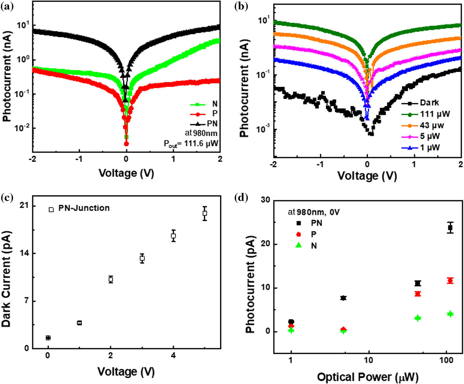
    Fig. 2. Photovoltaic characteristics of p-n-InSe heterojunction. (a) Typical IV characteristics of p (red), n (green), and p-n junction (black) 2D InSe photodetectors. (b) The IV characteristics of the p-n-InSe heterojunction under different optical input power show saturation of photocurrent at higher optical power. (c) Dark current mapping under bias voltage for p-n junction device indicates picoamps range current. This exhibits a noise equivalent power (NEP) of 2  nW/Hz0.5 at zero bias. (d) The corresponding fitting curves for the relationship between the photocurrents and the optical power of the p-InSe/n-InSe heterojunction under zero biased voltage and 980 nm light condition.
    Spectral characterization of p-n-InSe heterojunction. (a) Experimental spectra of responsivity of p-InSe, n-InSe, and p-n-InSe heterojunction at 0 V under 800–900 nm and 980 nm light illumination. (b) Photoluminescence spectra of p-InSe, n-InSe, and p-n-InSe heterojunction show strong agreement with the responsivity spectra. An enhancement of 4.5 times and 5.9 times in intensity is observed at 900 nm and 980 nm, respectively. (c) The quality of the heterojunction created was assessed at the A1g1 Raman peak at the physical position of the heterojunction region (white dashed region), as shown by Raman mapping analysis. A 532 nm laser was used for excitation.
    Fig. 3. Spectral characterization of p-n-InSe heterojunction. (a) Experimental spectra of responsivity of p-InSe, n-InSe, and p-n-InSe heterojunction at 0 V under 800–900 nm and 980 nm light illumination. (b) Photoluminescence spectra of p-InSe, n-InSe, and p-n-InSe heterojunction show strong agreement with the responsivity spectra. An enhancement of 4.5 times and 5.9 times in intensity is observed at 900 nm and 980 nm, respectively. (c) The quality of the heterojunction created was assessed at the A1g1 Raman peak at the physical position of the heterojunction region (white dashed region), as shown by Raman mapping analysis. A 532 nm laser was used for excitation.
    Time dependent photoresponse of (a) p-n-InSe photodetector at 0 V with rise time/fall time (τr/τf) of 8.3 ms/9.6 ms, (b) n-InSe at 2 V with τr/τf of 18 ms/40 ms, and (c) p-InSe at −2 V with τr/τf of 22 ms/29 ms. Under 980 nm light illumination.
    Fig. 4. Time dependent photoresponse of (a) p-n-InSe photodetector at 0 V with rise time/fall time (τr/τf) of 8.3 ms/9.6 ms, (b) n-InSe at 2 V with τr/τf of 18 ms/40 ms, and (c) p-InSe at 2  V with τr/τf of 22 ms/29 ms. Under 980 nm light illumination.
    Photoresponse mapping under external bias. (a) Photoresponse at different bias voltage (−2 to 2 V) with photocurrent of p-n-InSe under 980 nm illumination demonstrated the fastest response under 0 V bias condition. (b) Comparison of the photoresponse under the external bias of 2D photodetectors for NIR applications discussed in the literature.
    Fig. 5. Photoresponse mapping under external bias. (a) Photoresponse at different bias voltage (2 to 2 V) with photocurrent of p-n-InSe under 980 nm illumination demonstrated the fastest response under 0 V bias condition. (b) Comparison of the photoresponse under the external bias of 2D photodetectors for NIR applications discussed in the literature.
    Photograph of a p-InSe ingot cleaved parallel to the c-plane.
    Fig. 6. Photograph of a p-InSe ingot cleaved parallel to the c-plane.
    Atomic resolution annular dark-field scanning transmission electron microscopy (ADF-STEM) image of InSe showing a good match with the overlapped atomic model of γ-InSe. Green and purple dots in the atomic model represent Se and In atoms, respectively.
    Fig. 7. Atomic resolution annular dark-field scanning transmission electron microscopy (ADF-STEM) image of InSe showing a good match with the overlapped atomic model of γ-InSe. Green and purple dots in the atomic model represent Se and In atoms, respectively.
    2D printer transfer setup used for building the p-n heterojunction photodetector.
    Fig. 8. 2D printer transfer setup used for building the p-n heterojunction photodetector.
    Cross-sectional ADF-STEM image of the p-n-InSe photodetector fabricated using the 2D printer transfer setup.
    Fig. 9. Cross-sectional ADF-STEM image of the p-n-InSe photodetector fabricated using the 2D printer transfer setup.
    Materialsλ (nm)Responsivity (mA W-1)Bias Voltage (V)Idark (nA)τr/τf (ms/ms)Refs.
    InSe7003.06×10652005/8[20]
    Doped-InSe9807.87×10618000.45/6×103[27]
    Bi2Se31456274160054/47[42]
    BP/InSe633107010024/32[40]
    Gr/GaAs9805.9700.27540[13]
    Te/Ge9805220–5014/0.105[48]
    Ge bulk9802214–0.15[49]
    MoS2473−271247.514×10510/16[50]
    InGaAs1100–20003.5×1060.514470/280[51]
    p-n-InSe9800.501.5×1038.3/9.6This work
    Table 1. Comparison of the Performance of Our n-InSe/p-InSe Photodetector with Other NIR Photodetectors
    Chandraman Patil, Chaobo Dong, Hao Wang, Behrouz Movahhed Nouri, Sergiy Krylyuk, Huairuo Zhang, Albert V. Davydov, Hamed Dalir, Volker J. Sorger. Self-driven highly responsive p-n junction InSe heterostructure near-infrared light detector[J]. Photonics Research, 2022, 10(7): A97
    Download Citation