• Photonics Research
  • Vol. 8, Issue 9, 1506 (2020)
Yu Han1、2, Zhiguang Liu3, Shanshan Chen1, Juan Liu2、4、*, Yongtian Wang2, and Jiafang Li1、3、5、*
Author Affiliations
  • 1Key Laboratory of Advanced Optoelectronic Quantum Architecture and Measurement (Ministry of Education), Beijing Key Laboratory of Nanophotonics & Ultrafine Optoelectronic Systems, and School of Physics, Beijing Institute of Technology, Beijing 100081, China
  • 2Beijing Engineering Research Center for Mixed Reality and Advanced Display, School of Optics and Photonics, Beijing Institute of Technology, Beijing 100081, China
  • 3Institute of Physics, Chinese Academy of Sciences, Beijing 100190, China
  • 4e-mail: juanliu@bit.edu.cn
  • 5e-mail: jiafangli@bit.edu.cn
  • show less
    DOI: 10.1364/PRJ.398467 Cite this Article Set citation alerts
    Yu Han, Zhiguang Liu, Shanshan Chen, Juan Liu, Yongtian Wang, Jiafang Li. Cascaded multilayer nano-kirigami for extensible 3D nanofabrication and visible light manipulation[J]. Photonics Research, 2020, 8(9): 1506 Copy Citation Text show less
    Nano-kirigami on Au/SiN bilayer nanofilms. (a)–(c) Schematic illustration of nano-kirigami schemes by (a) FIB milling of a 2D pinwheel, (b) a 3D deformed pinwheel under FIB-based global irradiation, and (c) a 3D deformed pinwheel with flat central part under FIB-based Boolean-type irradiation. The wholly deformed pinwheel in (b) diffuses normally incident light, while the flat central plate in (c) reflects the light vertically under various deformed height, as noted by the red arrows. (d) Illustration of a four-layer pinwheel structure designed by cascaded FIB milling and Boolean irradiation.
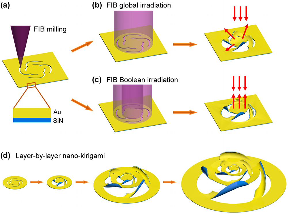
    Fig. 1. Nano-kirigami on Au/SiN bilayer nanofilms. (a)–(c) Schematic illustration of nano-kirigami schemes by (a) FIB milling of a 2D pinwheel, (b) a 3D deformed pinwheel under FIB-based global irradiation, and (c) a 3D deformed pinwheel with flat central part under FIB-based Boolean-type irradiation. The wholly deformed pinwheel in (b) diffuses normally incident light, while the flat central plate in (c) reflects the light vertically under various deformed height, as noted by the red arrows. (d) Illustration of a four-layer pinwheel structure designed by cascaded FIB milling and Boolean irradiation.
    (a), (b) SEM images of a pop-up plate structure fabricated by nano-kirigami on (a) an Au monolayer film and (b) an Au/SiN bilayer film. Insets show the zoom-in SEM image of the scanned line at the upper hinge. The inset of (a) shows a discontinuous boundary while the inset of (b) shows a clean cut and a smooth boundary. (c) A serial of gold plates isolated on a curved Au/SiN stripe. (d)–(h) (i) Designed and (ii) milled 2D patterns on Au/SiN bilayer films, as well as corresponding (iii) fabricated and (iv) calculated 3D nanostructures (with colors denoting the stress distributions), in different nano-kirigami schemes. (d) A symmetric flower-like structure under global irradiation. (e) A highly asymmetric three-arm pattern under global irradiation. (f) A three-arm pinwheel under global irradiation, showing curved deformation at the central part. (g) A three-arm pinwheel under Boolean irradiation, without any deformation in the central part. (h) A deformed mirror with three folded arms, with flat and large central part. The simulation results, with modified mechanical models, are in good agreement with the experimental results in all these five schemes. Scale bars: 1 μm.
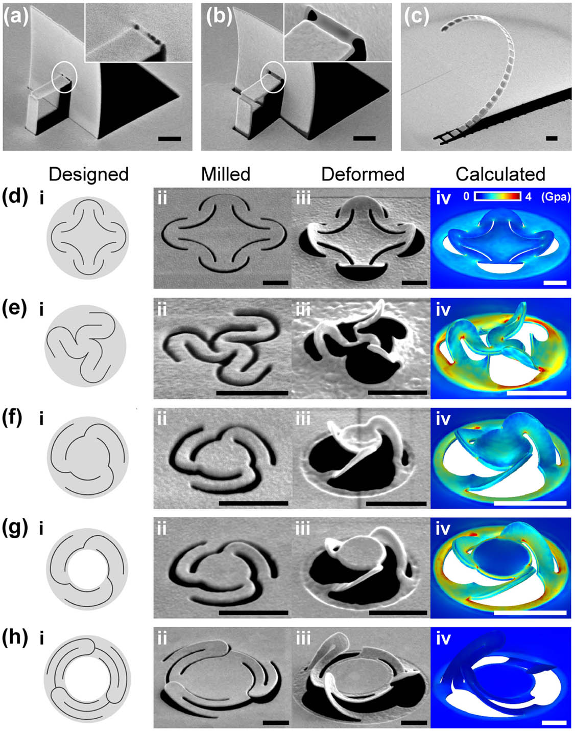
    Fig. 2. (a), (b) SEM images of a pop-up plate structure fabricated by nano-kirigami on (a) an Au monolayer film and (b) an Au/SiN bilayer film. Insets show the zoom-in SEM image of the scanned line at the upper hinge. The inset of (a) shows a discontinuous boundary while the inset of (b) shows a clean cut and a smooth boundary. (c) A serial of gold plates isolated on a curved Au/SiN stripe. (d)–(h) (i) Designed and (ii) milled 2D patterns on Au/SiN bilayer films, as well as corresponding (iii) fabricated and (iv) calculated 3D nanostructures (with colors denoting the stress distributions), in different nano-kirigami schemes. (d) A symmetric flower-like structure under global irradiation. (e) A highly asymmetric three-arm pattern under global irradiation. (f) A three-arm pinwheel under global irradiation, showing curved deformation at the central part. (g) A three-arm pinwheel under Boolean irradiation, without any deformation in the central part. (h) A deformed mirror with three folded arms, with flat and large central part. The simulation results, with modified mechanical models, are in good agreement with the experimental results in all these five schemes. Scale bars: 1 μm.
    (a) SEM images of a multilayer four-arm pinwheel structure fabricated from inner layer to outer layer. Each layer of the pinwheel is fabricated by FIB milling and subsequent low-dose Boolean irradiation. The FIB irradiation at the outer ring has no influence on the prior inner pattern, which makes possible the “unlimited” multilayer stacking in the vertical direction. (b), (c) Top-view and oblique-view SEM images of a multilayer pinwheel structure fabricated from outer to inner parts, resulting in the same four-layer pinwheel structure as in (a). (d) Calculated image of the multilayer pinwheel structure with the original mechanical model. The non-irradiated annular areas of multilayer pinwheels show severe local distortions as noted by the dashed circles, which are not consistent with the experimental results in (c). (e) Calculated image of the multilayer pinwheel structure with the modified mechanical model under the consideration of modulus softening effects. The simulation nearly perfectly reproduces the experimental observation in (c), verifying the accuracy and robustness of both the theoretical model and fabrication method. Scale bars: 1 μm.
    Fig. 3. (a) SEM images of a multilayer four-arm pinwheel structure fabricated from inner layer to outer layer. Each layer of the pinwheel is fabricated by FIB milling and subsequent low-dose Boolean irradiation. The FIB irradiation at the outer ring has no influence on the prior inner pattern, which makes possible the “unlimited” multilayer stacking in the vertical direction. (b), (c) Top-view and oblique-view SEM images of a multilayer pinwheel structure fabricated from outer to inner parts, resulting in the same four-layer pinwheel structure as in (a). (d) Calculated image of the multilayer pinwheel structure with the original mechanical model. The non-irradiated annular areas of multilayer pinwheels show severe local distortions as noted by the dashed circles, which are not consistent with the experimental results in (c). (e) Calculated image of the multilayer pinwheel structure with the modified mechanical model under the consideration of modulus softening effects. The simulation nearly perfectly reproduces the experimental observation in (c), verifying the accuracy and robustness of both the theoretical model and fabrication method. Scale bars: 1 μm.
    (a) Schematic illustration of (top) a 2D pinwheel with ring-shaped Boolean irradiation area and (bottom) the resulted 3D deformed pinwheel with a flat central plate. (b) Front view of the 3D deformed pinwheel with flat central plate of different height (h). The rising height induces a reflection phase shift of Δϕ with respect to the bottom layer under normal incidence of light. The maximum reachable height is determined by the geometric design, for example, the designed arm lengths. (c) Simulated phase distribution in reflection induced by the central plate at 11 different heights. Plane waves with λ=633, 532, and 473 nm are polarized along the x-axis direction. (d) (left) Height of the central plate and (right) corresponding Δϕ at the three wavelengths as functions of the prescribed deformation stress. The phase shift is obtained from (c), where the 11 states correspond to the 11 stresses applied in (d). (e) Intensity distribution of electric field in the xy plane (z=2 μm) for a 3×3 pinwheel array with h=122 nm and λ=532 nm (corresponding to Δϕ=π). (f) Normalized intensity distribution of electric field in the xz plane (y=0) for a deformed pinwheel with h=122 nm and λ=473, 532, and 633 nm, respectively. Periodic boundary conditions are applied in simulations.
    Fig. 4. (a) Schematic illustration of (top) a 2D pinwheel with ring-shaped Boolean irradiation area and (bottom) the resulted 3D deformed pinwheel with a flat central plate. (b) Front view of the 3D deformed pinwheel with flat central plate of different height (h). The rising height induces a reflection phase shift of Δϕ with respect to the bottom layer under normal incidence of light. The maximum reachable height is determined by the geometric design, for example, the designed arm lengths. (c) Simulated phase distribution in reflection induced by the central plate at 11 different heights. Plane waves with λ=633, 532, and 473 nm are polarized along the x-axis direction. (d) (left) Height of the central plate and (right) corresponding Δϕ at the three wavelengths as functions of the prescribed deformation stress. The phase shift is obtained from (c), where the 11 states correspond to the 11 stresses applied in (d). (e) Intensity distribution of electric field in the xy plane (z=2  μm) for a 3×3 pinwheel array with h=122  nm and λ=532  nm (corresponding to Δϕ=π). (f) Normalized intensity distribution of electric field in the xz plane (y=0) for a deformed pinwheel with h=122  nm and λ=473, 532, and 633 nm, respectively. Periodic boundary conditions are applied in simulations.
    Yu Han, Zhiguang Liu, Shanshan Chen, Juan Liu, Yongtian Wang, Jiafang Li. Cascaded multilayer nano-kirigami for extensible 3D nanofabrication and visible light manipulation[J]. Photonics Research, 2020, 8(9): 1506
    Download Citation