Abstract
Nano-kirigami enables direct and versatile shape transformations from two-dimensional predesigns to three-dimensional (3D) architectures in microscale/nanoscale. Here a new and extensible strategy for cascaded multilayer nano-kirigami is demonstrated in a gold/silicon nitride (Au/SiN) bilayer nanofilm for 3D nanofabrication and visible light manipulation. By employing a focused ion-beam-based Boolean irradiation, rich 3D shape transformation and nested multilayer nanostructures are precisely manufactured, which are well reproduced by developing a modified mechanical model. Based on the multilayer and deformable features of the nano-kirigami structures, potentials in manipulating the phase and intensity of visible light are explored. The developed new nano-kirigami strategies, as well as the novel exotic 3D nanostructures, could be helpful to build a novel platform for 3D nanofabrication and find potential applications in microelectromechanical/nanoelectromechanical systems, holographic display, plasmonics, nanophotonics, biophotonics, etc.1. INTRODUCTION
Three-dimensional (3D) nanofabrication, aiming to produce 3D microstructures/nanostructures with versatile physical properties and desired functionalities, forms the basis of modern information technology. For example, the basic complementary metal-oxide semiconductor technologies employ the repetitive surface patterning with optical lithography and consequential removal of sacrificial layers for the 3D construction of integrated electronic circuits [1]. Similarly, two-dimensional (2D) electron-beam lithography and focused ion beam (FIB) milling have been widely employed in multilayer stacking/lithography for 3D nanomanufacturing [2–4]. Meanwhile, to achieve direct 3D nanofabrication, translational direct laser writing has been developed with polymer skeleton and subsequent material inversion [5]. More recently, unconventional kirigami and origami methods [6], which unify the art and science of cutting and folding flat 2D objects to create 3D geometries, have been developed as promising schemes for microfabrication/nanofabrication and have attracted much attention in frontier fields such as microelectromechanical/nanoelectromechanical systems (MEMSs/NEMSs) [7], biomedical devices [8,9], and mechanical and photonic materials [10–16]. Different from traditional 3D fabrication techniques, microscale/nanoscale kirigami/origami enables the direct shape transformation from 2D patterns to 3D architectures without the need of precise 3D translation in direct laser writing [5,17] or accurate alignment during indirect multilayer stacking [18]. As a result, the fabricated nanogeometries can be greatly enriched in a variety of material platforms, which have exhibited great potentials for the generation of exceptional mechanical, optical, electronic, and biological functionalities [6]. However, current kirigami/origami strategies are still under the preliminary development, in which the desirable extensibility for later integration has yet been explored.
To develop an extensible scheme for 3D complex nanofabrication and drive this technique toward the manipulation of visible light, here we introduce a new strategy for FIB-based multilayer nano-kirigami in a commercial silicon nitride (SiN) film window coated with gold thin film. By employing an FIB-based Boolean irradiation, multilayer and cascaded 3D pinwheels are realized, which demonstrate the extensible stacking of nano-kirigami structures in the out-of-plane direction and are consistently verified by a modified elastoplastic mechanical model. Importantly, the upper flat plates and deformable features of the 3D pinwheels provide great potentials in manipulation of both phase and intensity of visible light. The reported method and study could be helpful to build a novel platform for 3D nanofabrication and find potential applications in MEMSs/NEMSs, optical spectroscopy, nanophotonics, biophotonics, etc.
2. RESULTS AND DISCUSSIONS
A. Multilayer Nano-kirigami in Bilayer Nanofilms
The general FIB-based nano-kirigami [19] normally includes three procedures, i.e., the preparation of nanofilms (as the “nanopaper”), the cutting of nanopatterns with high-dose FIB (as the “nanoscissors”), and the 3D deformation of the 2D nanopatterns with low-dose FIB (as the “nanohand”). In the last procedure, two irradiation schemes can be adopted to induce deformations, namely, local irradiation and global irradiation [19]. While the local irradiation induced discontinuous boundaries (as in later content) and the uniform global irradiation induced deformation in all structural areas, here a Boolean-type FIB irradiation scheme is proposed for cascaded and multilayer nano-kirigami, as shown in Fig. 1. This scheme involves the controlled spatial deformation of the 2D nanostructure into 3D nanoarchitectures by FIB irradiation with deliberately designed irradiation strategies, which include non-irradiated, irradiated, or overlapped areas, as shown in Fig. 1(c). It is named as Boolean irradiation in order to differentiate it from the uniform global irradiation. As illustrated in Fig. 1(b), the global low-dose irradiation covers the whole sample area, which induces deformations across the overall sample, including the undesirable deformation in the central part. In such a case, it is challenging for subsequent extensible building of multilayer nanostructures with freely designed morphologies due to entirely deformed areas that turn the fabrication out of focus. Moreover, the wholly deformed structures deflect the normally incident light in all directions, especially for the short visible wavelengths. In comparison, with the proposed Boolean-irradiation scheme in Fig. 1(c), the final ring-shaped Boolean irradiation is designed through subtraction operation of the two concentric circles. As a result, the arm areas of the pinwheel are selectively deformed, while the central part remains flat for later process and applications [right in Fig. 1(c)]. This is very advantageous for extensible manufacturing of nanostructures with increased complexity and flexibility. For example, as shown in Fig. 1(d), a four-layer nested pinwheel structure is designed by on-site cascaded milling and ring-shaped irradiation. It is anticipated that the outer parts of each layer can be dynamically twisted and rotated during the irradiation process, while the inner parts are passively rotated and translated without shape changes. Moreover, such multilayer complex structures can be realized via programed milling and irradiation processes, which are extremely challenging for traditional 3D nanofabrication methods.
Sign up for Photonics Research TOC. Get the latest issue of Photonics Research delivered right to you!Sign up now
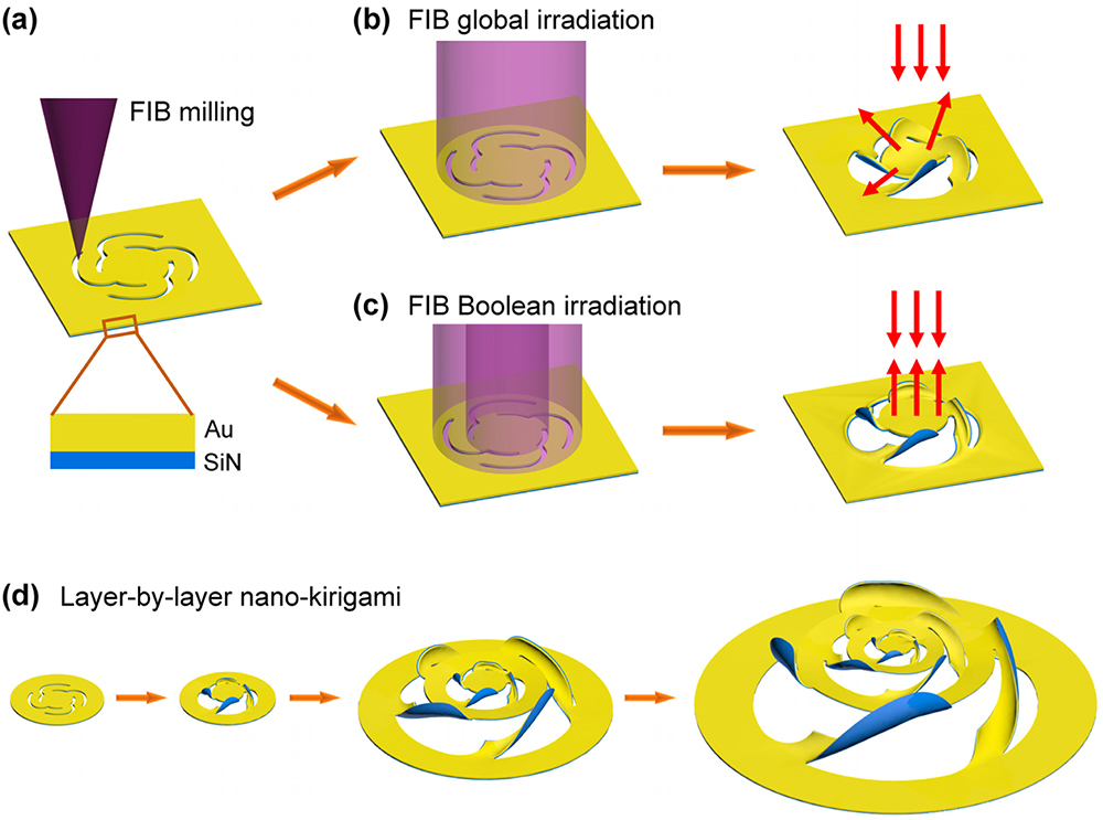
Figure 1.Nano-kirigami on Au/SiN bilayer nanofilms. (a)–(c) Schematic illustration of nano-kirigami schemes by (a) FIB milling of a 2D pinwheel, (b) a 3D deformed pinwheel under FIB-based global irradiation, and (c) a 3D deformed pinwheel with flat central part under FIB-based Boolean-type irradiation. The wholly deformed pinwheel in (b) diffuses normally incident light, while the flat central plate in (c) reflects the light vertically under various deformed height, as noted by the red arrows. (d) Illustration of a four-layer pinwheel structure designed by cascaded FIB milling and Boolean irradiation.
To implement the irradiation schemes, here we use a more general SiN film window (20 nm in thickness, Norcada Inc.) coated with 80-nm-thick gold film as the “nanopaper,” instead of the lift-off gold films suspended on copper grids [19,20]. The commercial SiN films are extremely flat, smooth, and easy-to-handle compared with the home-processed Au film that required sophisticated skills and time-consuming preparations. Meanwhile, the size of the SiN film window can be as large as , which is very advantageous for large-scale nanofabrication compared with that of Au film suspended on copper grids (normally with the flat area on the level of ). Moreover, by using Au/SiN bilayer film, the discontinuous boundary in Au monolayer film induced by FIB local irradiation can be overcome. As shown in Fig. 2(a), when the hinges of a pop-up plate structure are gradually thinned and folded, the hinge area gets rough and even broken due to the induced stress and the mobility of gold atoms during FIB irradiation, as in the inset of Fig. 2(a). This negative effect can be avoided in the Au/SiN bilayer film. As shown in the inset of Fig. 2(b), by controlling the dose of FIB irradiation, the gold atoms on the predesigned lines are completely removed from the film, and the bottom SiN layer remains as the smooth joint of the 3D nanostructure. Such clean boundary is very desirable to fabricate a series of isolated nanoparticles on curved SiN stripe, as illustrated in Fig. 2(c). It should be noted that compared with the fabrication on the Au monolayer, the FIB irradiation dosage required for the same fabrication was increased by when using the Au/SiN bilayer film.

Figure 2.(a), (b) SEM images of a pop-up plate structure fabricated by nano-kirigami on (a) an Au monolayer film and (b) an Au/SiN bilayer film. Insets show the zoom-in SEM image of the scanned line at the upper hinge. The inset of (a) shows a discontinuous boundary while the inset of (b) shows a clean cut and a smooth boundary. (c) A serial of gold plates isolated on a curved Au/SiN stripe. (d)–(h) (i) Designed and (ii) milled 2D patterns on Au/SiN bilayer films, as well as corresponding (iii) fabricated and (iv) calculated 3D nanostructures (with colors denoting the stress distributions), in different nano-kirigami schemes. (d) A symmetric flower-like structure under global irradiation. (e) A highly asymmetric three-arm pattern under global irradiation. (f) A three-arm pinwheel under global irradiation, showing curved deformation at the central part. (g) A three-arm pinwheel under Boolean irradiation, without any deformation in the central part. (h) A deformed mirror with three folded arms, with flat and large central part. The simulation results, with modified mechanical models, are in good agreement with the experimental results in all these five schemes. Scale bars: 1 μm.
To test the schemes in Fig. 1, various patterns are designed as in the first column of Figs. 2(d)–2(h). With the high accuracy of the FIB system (FEI Helios 600i), the designed patterns can be well reproduced on the bilayer film [the column (ii) of Figs. 2(d)–2(h)] by high-dose FIB milling (). It is important to note that the nano-kirigami method is a topography-guided 3D nanofabrication, that is, the final formation of 3D nanostructures is highly dependent on the topographic distribution of the stress in all subunits. Therefore, both structural designs and irradiation schemes are critical. In Fig. 2(d), for example, an axisymmetric flower-like structure with bended petals is fabricated, of which the central part cannot be deformed out of the plane by low-dose irradiation () due to the stresses destructively canceled at the center. In comparison, the nanostructure with rotational symmetry in Fig. 2(e) exhibits strong twisting and bending, indicating that the axial symmetry should be avoided to achieve dramatic twisting. Moreover, to increase the height of the deformed structures, a 3D pinwheel with three rotational arms is designed in Fig. 2(f), of which both the arms and central part are deformed under global FIB irradiation, agreeing well with the illustration in Fig. 1(b). In the case of Boolean irradiation, the same 2D pattern of Fig. 2(f) is irradiated by FIB under a ring-shaped area, as depicted in Fig. 2(g). It can be seen that besides the bending and twisting of the three arms, a smooth and flat plate in the center is preserved as in panel (iii) of Fig. 2(g), in a drastic contrast to that of Fig. 2(f). Moreover, the flat part of the pinwheel can be flexibly enlarged by specific designs, as the example shown in Fig. 2(h).
It should be mentioned that the structural stability during shape transformation needs careful considerations. It is found that when the structural size increases, the instability of the final deformation increases as well, such as the slightly tilted structure in panel (iii) of Fig. 2(h), as well as the reported spiral structures with only one leg connected to the master film [21]. Such a kind of instability is caused by the scanning direction and limited step of FIB systems. To address this limitation, the number of pinwheel supporters is increased. As shown in Fig. 3(a), the pinwheels with four supporting arms exhibit better stability in all scales.
Figure 3.(a) SEM images of a multilayer four-arm pinwheel structure fabricated from inner layer to outer layer. Each layer of the pinwheel is fabricated by FIB milling and subsequent low-dose Boolean irradiation. The FIB irradiation at the outer ring has no influence on the prior inner pattern, which makes possible the “unlimited” multilayer stacking in the vertical direction. (b), (c) Top-view and oblique-view SEM images of a multilayer pinwheel structure fabricated from outer to inner parts, resulting in the same four-layer pinwheel structure as in (a). (d) Calculated image of the multilayer pinwheel structure with the original mechanical model. The non-irradiated annular areas of multilayer pinwheels show severe local distortions as noted by the dashed circles, which are not consistent with the experimental results in (c). (e) Calculated image of the multilayer pinwheel structure with the modified mechanical model under the consideration of modulus softening effects. The simulation nearly perfectly reproduces the experimental observation in (c), verifying the accuracy and robustness of both the theoretical model and fabrication method. Scale bars: 1 μm.
With the aforementioned considerations, a scheme of cascaded multilayer nano-kirigami can be developed. As in Fig. 3(a), a multilayer four-arm pinwheel structure is realized from the inner layer to the outer layer (indicated by the horizontal arrow) by multiple high-dose milling and low-dose Boolean irradiation with FIB. During the fabrication, each annular exposed area is obtained by Boolean subtraction operation of two predesigned concentric circles. In such a case, the supporting arms of each layer bend and twist during the irradiation process, while the central parts are merely rotated and translated passively without local deformation, showing obviously the topographic characteristic of the nano-kirigami and overwhelming the global irradiation scheme regarding the structural complexity and flexibility. Moreover, the multilayer nano-kirigami structure can also be fabricated from the outer to the inner layer, as shown in Figs. 3(b) and 3(c). In this case, the supporting arms of the outer layers were bent and twisted during the low-dose irradiation process after the milling in each layer, while the inner unprocessed parts were translated vertically as the next layer for subsequent milling and Boolean irradiation (the ion beams need to be re-focused on each vertically shifted layer during the milling and annular irradiation). Such observations clearly prove the robustness of the Boolean-irradiation scheme and extensibility of such 3D nanofabrication (i.e., the number of layers can be increased on demand). Furthermore, these 3D exotic nanostructures have not been seen with the traditional nanofabrication techniques or the other kirigami methods, which could greatly enrich the variety of 3D nanogeometries in both designs and fabrications.
B. Theoretical Modeling of Complex Nano-kirigami Geometries
The accurate modeling of the complex nano-kirigami geometries is crucial for structural design and functionality prediction. To this end, a fundamental understanding of the nano-kirigami process is necessary. It is known that when energetic Ga ion beam bombards the thin film, some gallium atoms are implanted into the film, some gold atoms are sputtered away from the surface, some gold atoms within the film are dislocated, and some gold and gallium atoms re-deposit onto the surface [22–25]. These cascaded displacements caused by knock-on events introduce complicated stresses and strains across the film (defined as ) [19–22], which determine the structural formation through the following equations with zero net force () and net moment () across the film by [22] where is the sample thickness. Therefore, the distribution of local stress is critical. Previous studies with global irradiation simplified the free-standing Au film with a bilayer mechanical model [19], in which tensile stress concentrates in the top amorphous layer and passive deformation occurs in the bottom layer. Specifically, the residual stress distribution in the model can be described by [19]
Here, is the coordinate in the thickness direction; and are the thicknesses of the top plastic-deformation layer and the bottom elastoplastic-deformation layer, respectively. and are the residual stress in the top and bottom layers, respectively. and are the first- and second-order coefficients in the asymptotic expansion of stress in the bottom layer, with higher-order terms discarded due to the ultra-small thickness of the films. However, when the scheme of Boolean irradiation is adopted, the increased boundaries with such a model cause complications and even deviations in simulations. For example, the non-irradiated annular areas of multilayer pinwheels show severe local deformations when Eq. (2) is merely employed, as noted by the circles in Fig. 3(d), which deviate from the actual case in Figs. 3(a) and 3(c). This could be caused by an overlooked effect in which FIB irradiation on thin films can result in the softening effect of Young’s modulus [26]. To address these issues, we hereby develop a modified model by incorporating the bilayer model with modulus softening effects. In this modified model, the distribution of elastic modulus for all involved materials is determined by where and are the Young’s modulus of the corresponding bulk materials, respectively. The parameter (smaller than one) is used to define the extent of the modulus softening of the exposed Au layer upon the FIB irradiation. By adopting such a modified model in simulations with the finite element method, the four-layer nano-kirigami structure in Fig. 3(e) is directly calculated in one step and matches perfectly with the experimental results in Figs. 3(a) and 3(c), proving the robustness and accuracy of both experiments and calculations. Moreover, the versatile experimental nanostructures in the column (iii) of Fig. 2 are well reproduced by the numerical simulations in the column (iv) of Fig. 2. These observations clearly prove that the prescribed 2D patterns of various geometries can result in dramatically different 3D configurations under the topography-guided stress equilibrium.
C. Potential Applications of Nano-kirigami at Visible Wavelengths
The versatile geometries realized by nano-kirigami represent a new type of nanophotonic structures. For example, benefiting from the flatness of the central part during the Boolean-type FIB irradiation, as illustrated in Fig. 4(a), the pinwheels with deformable height can be employed to manipulate the phase and intensity of visible light. As schematically shown in Fig. 4(b), when the central plate rises with a height of with respect to the bottom layer, an extra reflection phase shift () will be introduced under normal incidence [Fig. 4(c)]. For example, when the pinwheel is exerted by different prescribed stress, the height of its central plate increases correspondingly with a nearly linear relation, as plotted in the left of Fig. 4(d), resulting in a height of 222 nm under (in Au film). Meanwhile, the reflection phase distribution at different states varies in a different manner, as the finite-difference time-domain simulation results for the red (633 nm), green (532 nm), and blue (473 nm) wavelengths shown in Fig. 4(c). It can be clearly seen that the generated phase shift varies from 0 to nearly , as plotted in the right of Fig. 4(d). It should be mentioned that the slopes of the curves vary with different wavelengths since , where is the effective refractive index of the medium and is the operating wavelength.
Figure 4.(a) Schematic illustration of (top) a 2D pinwheel with ring-shaped Boolean irradiation area and (bottom) the resulted 3D deformed pinwheel with a flat central plate. (b) Front view of the 3D deformed pinwheel with flat central plate of different height (h). The rising height induces a reflection phase shift of with respect to the bottom layer under normal incidence of light. The maximum reachable height is determined by the geometric design, for example, the designed arm lengths. (c) Simulated phase distribution in reflection induced by the central plate at 11 different heights. Plane waves with , 532, and 473 nm are polarized along the -axis direction. (d) (left) Height of the central plate and (right) corresponding at the three wavelengths as functions of the prescribed deformation stress. The phase shift is obtained from (c), where the 11 states correspond to the 11 stresses applied in (d). (e) Intensity distribution of electric field in the plane () for a pinwheel array with and (corresponding to ). (f) Normalized intensity distribution of electric field in the plane () for a deformed pinwheel with and , 532, and 633 nm, respectively. Periodic boundary conditions are applied in simulations.
Since the heights of the pinwheels are potentially tunable under dynamic electrostatic or mechanical forces [27,28], the large-range phase engineering in Figs. 4(c) and 4(d) could provide a useful approach for the manipulation of visible light. To test the feasibility, an array of the deformed pinwheels with is arranged in a square lattice with periodicity of 2 μm. As shown in Fig. 4(e), a strong interference pattern is clearly formed at under normal incidence. Such an interference pattern is highly dependent on the height of the deformed pinwheels and varies significantly with wavelength since , as plotted in Fig. 4(f). Therefore, the deformable features of the nano-kirigami structures make it promising for the dynamic modulation of visible light through reconfiguring their heights, which could provide a novel methodology for efficient beam steering employed in optical displays and light/laser radar systems.
3. CONCLUSIONS
In summary, we have demonstrated an efficient method to fabricate exotic 3D nano-kirigami nanostructures. Based on a systematic consideration from the aspects of fabrication sequences, structural symmetry, and extensible integration, cascaded multilayer nano-kirigami structures have been realized under Boolean-type FIB irradiation, which are highly extendable in the out-of-plane direction and widely applicable in commercial Au/SiN bilayer nanofilms for large-scale manufacturing. The 3D complex structures have been well reproduced by developing a modified elastoplastic mechanical model that included the softening of material modulus, which provides a reliable guidance for the design and prediction of desirable functionalities. Moreover, the engineering of phase and intensity by nano-kirigami structures has been numerically demonstrated by employing the deformed pinwheels with deliberately designed height. Therefore, our work paves a new way for fabricating sophisticated and complex 3D nanostructures for advanced photonic applications in beam steering, optical reconfiguration, holographic displays, metasurface devices, MEMSs/NEMSs, optical sensors, optomechanical devices, etc.
Acknowledgment
Acknowledgment. The authors thank Laboratory of Microfabrication, Institute of Physics, CAS for assistance in FIB facilities and useful discussions.
References
[1] R. Syms, E. Yeatman. Self-assembly of three-dimensional microstructures using rotation by surface tension forces. Electron. Lett., 29, 662-664(1993).
[2] F. Stellacci, C. A. Bauer, T. Meyer-Friedrichsen, W. Wenseleers, V. Alain, S. M. Kuebler, S. J. K. Pond, Y. D. Zhang, S. R. Marder, J. W. Perry. Laser and electron-beam induced growth of nanoparticles for 2D and 3D metal patterning. Adv. Mater., 14, 194-198(2002).
[3] F. De Angelis, C. Liberale, M. L. Coluccio, G. Cojoc, E. Di Fabrizio. Emerging fabrication techniques for 3D nano-structuring in plasmonics and single molecule studies. Nanoscale, 3, 2689-2696(2011).
[4] Y. Hong, D. Zhao, D. L. Liu, B. Z. Ma, G. N. Yao, Q. Li, A. P. Han, M. Qiu. Three-dimensional in situ electron-beam lithography using water ice. Nano Lett., 18, 5036-5041(2018).
[5] J. K. Gansel, M. Thiel, M. S. Rill, M. Decker, K. Bade, V. Saile, G. von Freymann, S. Linden, M. Wegener. Gold helix photonic metamaterial as broadband circular polarizer. Science, 325, 1513-1515(2009).
[6] S. Chen, J. Chen, X. Zhang, Z.-Y. Li, J. Li. Kirigami/origami: unfolding the new regime of advanced 3D microfabrication/nanofabrication with ‘folding’. Light Sci. Appl., 9, 75(2020).
[7] J. Rogers, Y. G. Huang, O. G. Schmidt, D. H. Gracias. Origami MEMS and NEMS. Mrs Bull., 41, 123-129(2016).
[8] K. Kuribayashi, K. Tsuchiya, Z. You, D. Tomus, M. Umemoto, T. Ito, M. Sasaki. Self-deployable origami stent grafts as a biomedical application of Ni-rich TiNi shape memory alloy foil. Mater. Sci. Eng. A, 419, 131-137(2006).
[9] C. Yang, H. Zhang, Y. D. Liu, Z. L. Yu, X. D. Wei, Y. F. Hu. Kirigami-inspired deformable 3D structures conformable to curved biological surface. Adv. Sci., 5, 1801070(2018).
[10] A. Lamoureux, K. Lee, M. Shlian, S. R. Forrest, M. Shtein. Dynamic kirigami structures for integrated solar tracking. Nat. Commun., 6, 8092(2015).
[11] M. K. Blees, A. W. Barnard, P. A. Rose, S. P. Roberts, K. L. McGill, P. Y. Huang, A. R. Ruyack, J. W. Kevek, B. Kobrin, D. A. Muller, P. L. McEuen. Graphene kirigami. Nature, 524, 204-207(2015).
[12] Z. J. Wang, L. Q. Jing, K. Yao, Y. H. Yang, B. Zheng, C. M. Soukoulis, H. S. Chen, Y. M. Liu. Origami-based reconfigurable metamaterials for tunable chirality. Adv. Mater., 29, 1700412(2017).
[13] J. L. Silverberg, A. A. Evans, L. McLeod, R. C. Hayward, T. Hull, C. D. Santangelo, I. Cohen. Using origami design principles to fold reprogrammable mechanical metamaterials. Science, 345, 647-650(2014).
[14] Y. S. Guan, Z. L. Zhang, Y. C. Tang, J. Yin, S. Q. Ren. Kirigami-inspired nanoconfined polymer conducting nanosheets with 2000% stretchability. Adv. Mater., 30, 1801070(2018).
[15] L. Z. Xu, T. C. Shyu, N. A. Kotov. Origami and kirigami nanocomposites. ACS Nano, 11, 7587-7599(2017).
[16] W. J. Choi, G. Cheng, Z. Y. Huang, S. Zhang, T. B. Norris, N. A. Kotov. Terahertz circular dichroism spectroscopy of biomaterials enabled by kirigami polarization modulators. Nat. Mater., 18, 820-826(2019).
[17] M. D. Turner, M. Saba, Q. M. Zhang, B. P. Cumming, G. E. Schroder-Turk, M. Gu. Miniature chiral beamsplitter based on gyroid photonic crystals. Nat. Photonics, 7, 801-805(2013).
[18] C. Q. Zheng, Y. Shen, M. K. Liu, W. J. Liu, S. Y. Wu, C. J. Jin. Layer-by-layer assembly of three dimensional optical functional nanostructures. ACS Nano, 13, 5583-5590(2019).
[19] Z. Liu, H. Du, J. Li, L. Lu, Z.-Y. Li, N. X. Fang. Nano-kirigami with giant optical chirality. Sci. Adv., 4, eaat4436(2018).
[20] A. J. Cui, Z. Liu, J. F. Li, T. H. H. Shen, X. X. Xia, Z. Y. Li, Z. J. Gong, H. Q. Li, B. L. Wang, J. J. Li, H. F. Yang, W. X. Li, C. Z. Gu. Directly patterned substrate-free plasmonic ‘nanograter’ structures with unusual Fano resonances. Light Sci. Appl., 4, e308(2015).
[21] M. L. Tseng, Z. H. Lin, H. Y. Kuo, T. T. Huang, Y. T. Huang, T. L. Chung, C. H. Chu, J. S. Huang, D. P. Tsai. Stress-induced 3D chiral fractal metasurface for enhanced and stabilized broadband near-field optical chirality. Adv. Opt. Mater., 7, 1900617(2019).
[22] W. J. Arora, H. I. Smith, G. Barbastathis. Membrane folding by ion implantation induced stress to fabricate three-dimensional nanostructures. Microelectron. Eng., 84, 1454-1458(2007).
[23] C. L. Wu, F. C. Li, C. W. Pao, D. J. Srolovitz. Folding sheets with ion beams. Nano Lett., 17, 249-254(2017).
[24] W. D. Nix, B. M. Clemens. Crystallite coalescence: a mechanism for intrinsic tensile stresses in thin films. J. Mater. Res., 14, 3467-3473(1999).
[25] M. J. Samayoa, M. A. Haque, P. H. Cohen. Focused ion beam irradiation effects on nanoscale freestanding thin films. J. Micromech. Microeng., 18, 095005(2008).
[26] A. Battiato, M. Lorusso, E. Bernardi, F. Picollo, F. Bosia, D. Ugues, A. Zelferino, A. Damin, J. Baima, N. M. Pugno, E. P. Ambrosio, P. Olivero. Softening the ultra-stiff: controlled variation of Young’s modulus in single-crystal diamond by ion implantation. Acta Mater., 116, 95-103(2016).
[27] S. Chen, Z. Liu, H. Du, C. Tang, C. Ji, B. Quan, R. Pan, L. Yang, X. Li, C. Gu, X. Zhang, Y. Yao, J. Li, N. X. Fang, J. Li. Electromechanically reconfigurable optical nano-kirigami. Nat. Commun..
[28] Z. G. Liu, Y. Xu, C. Y. Ji, S. S. Chen, X. P. Li, X. D. Zhang, Y. G. Yao, J. F. Li. Fano-enhanced circular dichroism in deformable stereo metasurfaces. Adv. Mater., 32, 1907077(2020).

