
Ye YUAN, Xiang-Bin SU, Cheng-ao YANG, Yi ZHANG, Jin-Ming SHANG, Sheng-Wen XIE, Yu ZHANG, Hai-Qiao NI, Ying-Qiang XU, Zhi-Chuan NIU. Molecular beam epitaxial growth of InAs quantum dots on GaAs for high characteristics temperature lasers[J]. Journal of Infrared and Millimeter Waves, 2020, 39(6): 667
- Journal of Infrared and Millimeter Waves
- Vol. 39, Issue 6, 667 (2020)
Abstract
Introduction
In recent years, 1.3 μm quantum dot(QD) laser has become an important light source for optical communication.[
The device characteristics of quantum dot laser are mainly limited by the growth conditions of the active region. To obtain better performance quantum dot laser, the growth temperature of the active region was optimized, and Be-doping in the active region was introduced for better temperature characteristics. We will show the fabrication of high characteristic temperature with low threshold current density single emitter diode laser device with 100 μm-wide and 2 mm-long cavity. The peak power of quantum dot laser reached 1008 mW. The threshold current density is 110 A/cm2, and the characteristic temperature below 50 ℃ is 405 K by fitting the curve between threshold current and temperature.
1 Structure characterization and fabrication
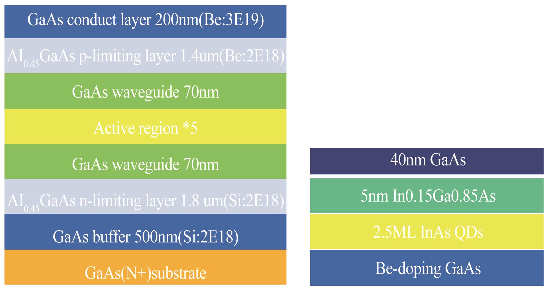
The quantum dot laser structure shown in the Fig. 1 was grown on N-type GaAs (100) substrates exploiting a Gen 930 solid-source Molecular beam epitaxy(MBE) system from Veeco Instruments equipped with in-situ reflective high-energy electron diffractometer (RHEED) calibrating the growth temperature by the GaAs reconstruction.[
![]()
Figure 1.The structure of the QD laser and the structure of the active region
The growth temperature of the QD is the vital parameter in the MBE epitaxy of the laser. At lower temperature, the density of quantum dots is the highest, but the uniformity is not enough, and it is easy to form large dot defects. The uniformity of quantum dots is better at higher growth temperature, but the high growth temperature will lead to the desorption of InAs quantum dots, which will lead to the decrease of the quantum dots density. To find the optimized growth temperature of the QDs, photoluminescence(PL) spectrum and atomic force microscope(AFM) were carried out on three QDs samples with the growth temperature of 510 ℃,520 ℃ and 530 ℃. All the PL spectra shown in Fig. 2 were obtained with a Fourier transform infrared spectroscopy (FTIR) by detecting the PL signals excited by a 500 mW 628 nm diode laser, and it is obvious that the sample grown at 520 ℃ has the best optical quality among the three samples. As indicated in Fig.3, the sample grown at 510 ℃ has several large dots defects which will deteriorate the performance of the device, and the density of quantum dots of the sample grown at 530 ℃ is the lowest which led to lower optical quality. The growth temperature was finally optimized to 520 ℃,and the full width at half maximum (FWHM) is 35 nm and the density of the QDs is 5.0×1010 cm-2.
![]()
Figure 2.PL spectrum of the three QDs samples with growth temperature of 510℃,520℃ and 530℃
![]()
Figure 3.Atomic force microscope (AFM)image of the three QDs samples (a)510 ℃,(b)520 ℃, and (c)530 ℃)
The grown epitaxial wafers were processed into diode laser with a ridge waveguide of 100 μm wide, 2 mm long and 1.5 μm deep using contact optical lithography followed by inductively coupled plasma (ICP) dry etching. Then 90 μm wide, 1.9mm-long electrode aperture was open using ICP etching on the 200 nm SiO2 insulation layer deposited by PECVD. After that, the p-side Ti/Pt/Au electrode was formed by magnetism sputter system. The n-side Ohm contacts were realized by fast-annealing the evaporated AuGeNi/Au film after the wafers were thinned to 150 μm. Finally, the wafers were cleaved into single emitter, and all the laser devices were mounted p-side down on copper heat sinks with Indium solder.
2 Laser performance and discussion
All the laser performance was measured without facet coating. The measurements of lasers output power were done by a pyroelectric detector and the emission spectra were scanned using a Fourier transform infrared spectroscopy (FTIR) system. The Continuous wave power-current-Voltage(P-I-V) characteristics and wall plug efficiency(WPE) at RT is shown in Fig.4, and the maximal output power reaches 1 008 mW at the injection current of 3.6 A, then as the current increased further the output power was limited for the reason of heat accumulation. The threshold current density is 110 A/cm2 and the WPE is 29%. The central wavelength of the lasing spectrum is 1.3 μm shown in Fig.5. Due to p-doping in the active region, the impurity atoms provide a lot of extra holes to fill the valence band energy level of the quantum dots, which makes the valence band energy level always in the state of filling. It is difficult for the ground state holes to escape from the heat, which improves the probability of the ground state carrier occupation of the valence band, and thus improves the characteristic temperature of the quantum dot laser.[
![]()
Figure 4.
![]()
Figure 5.Lasing spectrum at RT (The central wavelength is 1.3 μm)
![]()
Figure 6.The power-current(
3 Conclusion
In conclusion, we obtained 1.3 μm QD laser operating at room temperature with high characteristic temperature based on the optimization of the growth temperature and proper Be-doping in the active region. The uncoated facet single-emitter laser devices which had 100 μm-wide and 2 mm-long cavity with threshold current density of 110 A/cm2 were fabricated. For each single quantum dots layer, the threshold current density is as low as 22 A/cm2. The peak power of quantum dot laser reached 1008 mW at the injection current of 3.6 A. The highest continuous wave operating temperature is 80 ℃, and the characteristic temperature is 405 K by fitting the curve between threshold current and temperature.
References
[1] Y Tanaka, M Ishida, Y Maeda, et al. 2009 San Diego, United States, p. OWJ1. March 22(26).
[3] Z Wang, S Preble, C S Lee. 2015 Proceedings of Advanced Photonics: Integrated Photonics Research, Silicon and Nanophotonics, June 27–July 1, 2015 Boston, United States, p. IM4B(4).
[5] H Y Liu, I R Sellers, M Gutiérrez. Optimizing the growth of 1.3-μm InAs/InGaAs dots-in-a-well structure: Achievement of high-performance laser. Materials Science & Engineering C, 5, 779-783(25).
[6] H Heidemeyer, C Müller, O G Schmidt. Highly ordered arrays of In(Ga)As quantum dots on patterned GaAs(001) substrates. Journal of Crystal Growth, 261, 444-449(2004).
[7] H M Hao, X B Su, J Zhang. Molecular beam epitaxial growth of high quality InAs/GaAs quantum dots for 1.3-μm quantum dot lasers. Chin. Phys. B, 28, 078104(2019).
[8] Y Cao, T Yang, H Ji. Temperature sensitivity dependence on cavity length in p-type doped and undoped 1.3-μm InAs–GaAs quantum-dot lasers. IEEE Photonics Technology Letters, 20, 1860-1862(2008).
[9] K Otsubo, N Hatori, M Ishida. Temperature-insensitive eye-opening under 10-Gb/s modulation of 1.3-μm P-doped quantum-dot lasers without current adjustments. Japanese Journal of Applied Physics, 43, L1124-L1126(2004).
[10] V M Ustinov, N A Maleev, A E Zhukov. InAs/InGaAs quantum dot structures on GaAs substrates emitting at 1.3 μm. Applied Physics Letters, 74, 2815-2817(1999).
[11] F H Shao, Y Zhang, X B Su. 1.3-μm InAs/GaAs quantum dots grown on Si substrates. Chin. Phys. B, 27, 128105(2018).
[12] V M Ustinov, N A Maleev, A E Zhukov. InAs/InGaAs quantum dot structures on GaAs substrates emitting at 1.3 μm. Applied Physics Letters, 74, 2815-2817(1999).
[13] O Shchekin, J Ahn, D Deppe. High temperature performance of self-organised quantum dot laser with stacked p-doped active region. Electronics Letters, 38, 712-713(2002).
[14] Q Cao, S F Yoon, C Y Liu. Effects of rapid thermal annealing on optical properties of p-doped and undoped InAs/InGaAs dots-in-a-well structures. Journal of Applied Physics, 104, 033522(2008).
[15] S M Kim, Y Wang, M Keever. High-frequency modulation characteristics of 1.3-μm InGaAs quantum dot lasers. IEEE Photonics Technology Letters, 16, 377-379(2004).
[16] C Y Liu, S F Yoon, Q Cao. Low transparency current density and high temperature operation from ten-layer p-doped 1.3μm InAs∕InGaAs∕GaAs quantum dot lasers. Applied Physics Letters, 90, 227(2007).
[17] R Murray, D Childs, S Malik. 1.3 μm room temperature emission from InAs/GaAs Self-assembled quantum dots. Japanese Journal of Applied Physics, 38, 528-530(1999).
[18] D G Deppe, H Huang, O B Shchekin. Modulation characteristics of quantum-dot lasers: the influence of p-type doping and the electronic density of states on obtaining high speed. IEEE Journal of Quantum Electronics, 38, 1587-1593(2002).

Set citation alerts for the article
Please enter your email address
© Copyright 2018-2021 | Chinese Laser Press. All Rights Reserved 沪ICP备15018463号-20