• Advanced Photonics
  • Vol. 4, Issue 3, 034003 (2022)
Guanyu Chen1, Nanxi Li2, Jun Da Ng1, Hong-Lin Lin1, Yanyan Zhou2, Yuan Hsing Fu2, Lennon Yao Ting Lee2, Yu Yu3、*, Ai-Qun Liu4, and Aaron J. Danner1、*
Author Affiliations
  • 1National University of Singapore, Department of Electrical and Computer Engineering, Singapore
  • 2A*STAR (Agency for Science, Technology and Research), Institute of Microelectronics, Singapore
  • 3Huazhong University of Science and Technology, School of Optical and Electronic Information, Wuhan National Laboratory for Optoelectronics, Wuhan, China
  • 4Nanyang Technological University, Quantum Science and Engineering Centre, Singapore
  • show less
    DOI: 10.1117/1.AP.4.3.034003 Cite this Article Set citation alerts
    Guanyu Chen, Nanxi Li, Jun Da Ng, Hong-Lin Lin, Yanyan Zhou, Yuan Hsing Fu, Lennon Yao Ting Lee, Yu Yu, Ai-Qun Liu, Aaron J. Danner. Advances in lithium niobate photonics: development status and perspectives[J]. Advanced Photonics, 2022, 4(3): 034003 Copy Citation Text show less
    Overview of LN photonics. Top middle inset is LN crystal structure. EO, electro-optic; SHG, second harmonic generation; SFG/DFG, sum/difference frequency generation; SCG, supercontinuum generation; OPA/OPO, optical parametric amplification/oscillation; SRS, stimulated Raman scattering; PPLN, periodically poled lithium niobate; GC, grating coupler; WL, wavelength; AO, acousto-optic.
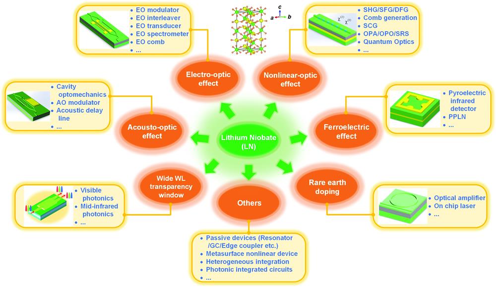
    Fig. 1. Overview of LN photonics. Top middle inset is LN crystal structure. EO, electro-optic; SHG, second harmonic generation; SFG/DFG, sum/difference frequency generation; SCG, supercontinuum generation; OPA/OPO, optical parametric amplification/oscillation; SRS, stimulated Raman scattering; PPLN, periodically poled lithium niobate; GC, grating coupler; WL, wavelength; AO, acousto-optic.
    Process flow of planar LN device fabrication. Illustration of (a) metal ion-in diffusion and (b) PE methods for planar photonic device fabrication in bulk LN crystals (dimensions are not drawn to scale). PR, photoresist.
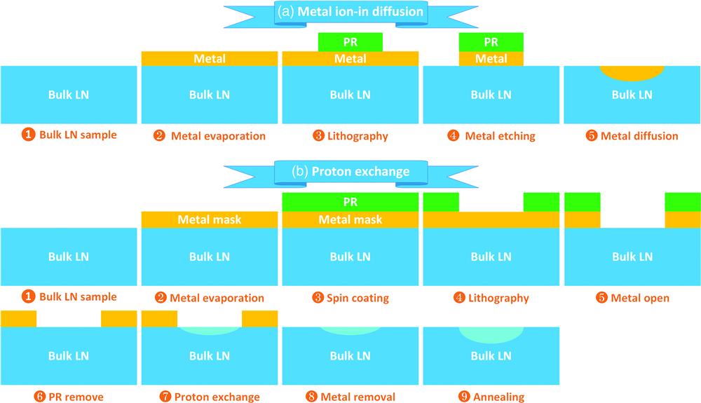
    Fig. 2. Process flow of planar LN device fabrication. Illustration of (a) metal ion-in diffusion and (b) PE methods for planar photonic device fabrication in bulk LN crystals (dimensions are not drawn to scale). PR, photoresist.
    Process flows of (a) CIS and (b) lapping and polishing technologies. Dimensions are not drawn to scale.
    Fig. 3. Process flows of (a) CIS and (b) lapping and polishing technologies. Dimensions are not drawn to scale.
    Heterogeneous integrated LN devices. (a) Schematic structure, (b) optical, and (c) atomic force microscopic images of an LN on silica hybrid micro-resonator. (a)–(c) Adapted from Ref. 161 © 2015 Wiley-VCH Verlag GmbH and Co. (d) 3D schematic structure, (e) cross section and optical field distribution of a SiNx on LN hybrid MZI modulator. (d) and (e) Adapted from Ref. 169; all article content, except where otherwise noted, is licensed under a Creative Commons Attribution (CC BY) license.
    Fig. 4. Heterogeneous integrated LN devices. (a) Schematic structure, (b) optical, and (c) atomic force microscopic images of an LN on silica hybrid micro-resonator. (a)–(c) Adapted from Ref. 161 © 2015 Wiley-VCH Verlag GmbH and Co. (d) 3D schematic structure, (e) cross section and optical field distribution of a SiNx on LN hybrid MZI modulator. (d) and (e) Adapted from Ref. 169; all article content, except where otherwise noted, is licensed under a Creative Commons Attribution (CC BY) license.
    Dry etching results of LN. (a) SEM image of the LN cross section and (b) current changed along etching depth in end point detection after SF6 based etching. (a) and (b) Adapted from Ref. 182 © 2008 American Institute of Physics (AIP). (c) SEM, (d) AFM, and (e) XPS images of LN sample after Ar-based dry etching. (c)–(e) Adapted with permission from Ref. 175.
    Fig. 5. Dry etching results of LN. (a) SEM image of the LN cross section and (b) current changed along etching depth in end point detection after SF6 based etching. (a) and (b) Adapted from Ref. 182 © 2008 American Institute of Physics (AIP). (c) SEM, (d) AFM, and (e) XPS images of LN sample after Ar-based dry etching. (c)–(e) Adapted with permission from Ref. 175.
    Wet etching results of LN. SEM images of the LN etched cross section using undiluted (a) 0% and (b) 20% of adipic acid, (c) 0% and (d) 20% of adipic acid with 0.6% of lithium benzoate, (e) 20% and (f) 30% of adipic acid with 0.3% of lithium carbonate (concentrations in percent represent mole fractions). (a)–(f) Adapted from Ref. 198 © 2006 Wiley Periodicals, Inc. (g) SEM image of photonic crystals (PhCs) using ion implantation and wet etching. Adapted with permission from Ref. 138 © 2010 American Vacuum Society.
    Fig. 6. Wet etching results of LN. SEM images of the LN etched cross section using undiluted (a) 0% and (b) 20% of adipic acid, (c) 0% and (d) 20% of adipic acid with 0.6% of lithium benzoate, (e) 20% and (f) 30% of adipic acid with 0.3% of lithium carbonate (concentrations in percent represent mole fractions). (a)–(f) Adapted from Ref. 198 © 2006 Wiley Periodicals, Inc. (g) SEM image of photonic crystals (PhCs) using ion implantation and wet etching. Adapted with permission from Ref. 138 © 2010 American Vacuum Society.
    LN-based microresonators. (a) Schematic experimental setup for characterizing a mechanical polishing bulk LN whispering-gallery resonator and its corresponding measured Q factor. Adapted from Ref. 227 © 2011 AIP. (b) Resonance spectra of the fabricated microdisk using ECR RIE technology in TFLN. Inset shows the microscope image of tapered fiber coupling on top of the device. Zoom in views are the details of representative resonance dips. Adapted with permission from Ref. 228 © 2014 Optical Society of America (OSA). (c) SEM (top) and microscopic images (bottom) of microring and microracetrack ring with various lengths, and (d) its measured transmission spectrum. (c) and (d) Adapted with permission from Ref. 192 © 2017 OSA. (e) Microscope image of the waveguide coupled TFLN microring and (f) its measured transmission spectrum. The Q factors for (g) TE and (h) TM modes fitted by Lorentz-shape curves. (e)–(h) Adapted with permission from Ref. 224 © 2022 Chinese Optical Society (COS).
    Fig. 7. LN-based microresonators. (a) Schematic experimental setup for characterizing a mechanical polishing bulk LN whispering-gallery resonator and its corresponding measured Q factor. Adapted from Ref. 227 © 2011 AIP. (b) Resonance spectra of the fabricated microdisk using ECR RIE technology in TFLN. Inset shows the microscope image of tapered fiber coupling on top of the device. Zoom in views are the details of representative resonance dips. Adapted with permission from Ref. 228 © 2014 Optical Society of America (OSA). (c) SEM (top) and microscopic images (bottom) of microring and microracetrack ring with various lengths, and (d) its measured transmission spectrum. (c) and (d) Adapted with permission from Ref. 192 © 2017 OSA. (e) Microscope image of the waveguide coupled TFLN microring and (f) its measured transmission spectrum. The Q factors for (g) TE and (h) TM modes fitted by Lorentz-shape curves. (e)–(h) Adapted with permission from Ref. 224 © 2022 Chinese Optical Society (COS).
    LN-based GCs. (a) Schematic structure, (b) simulated electric field distribution and (c) measured transmission spectrum of 1D chirped GC in TFLN. (a)–(c) Adapted with permission from Ref. 259 © 2020 OSA. (d) Schematic structure of a 2D GC in TFLN. Measured and simulated (e) transmission spectra and (f) polarization dependence loss of the TFLN 2D GC. (d)–(f) Adapted with permission from Ref. 265 © 2021 OSA.
    Fig. 8. LN-based GCs. (a) Schematic structure, (b) simulated electric field distribution and (c) measured transmission spectrum of 1D chirped GC in TFLN. (a)–(c) Adapted with permission from Ref. 259 © 2020 OSA. (d) Schematic structure of a 2D GC in TFLN. Measured and simulated (e) transmission spectra and (f) polarization dependence loss of the TFLN 2D GC. (d)–(f) Adapted with permission from Ref. 265 © 2021 OSA.
    LN-based edge coupler. (a) Schematic structure of the bilayer edge coupler and its corresponding mode profiles at different positions. (b) Simulated and measured coupling efficiency versus different tip widths in the tapered slab region. (c) Additional insertion loss with respect to coupling misalignment (TE mode). (a)–(c) Adapted with permission from Ref. 246 © 2019 OSA.
    Fig. 9. LN-based edge coupler. (a) Schematic structure of the bilayer edge coupler and its corresponding mode profiles at different positions. (b) Simulated and measured coupling efficiency versus different tip widths in the tapered slab region. (c) Additional insertion loss with respect to coupling misalignment (TE mode). (a)–(c) Adapted with permission from Ref. 246 © 2019 OSA.
    TFLN EO tunable microring resonator. (a) Schematic structure (top), cross section (bottom left), and SEM images of the Z-cut TFLN microring modulator, and (b) its EO resonance shift curve. (a) and (b) Adapted with permission from Ref. 181 © 2007 Nature Publishing Group.
    Fig. 10. TFLN EO tunable microring resonator. (a) Schematic structure (top), cross section (bottom left), and SEM images of the Z-cut TFLN microring modulator, and (b) its EO resonance shift curve. (a) and (b) Adapted with permission from Ref. 181 © 2007 Nature Publishing Group.
    TFLN-based modulators. (a) Microscopic image of TFLN MZI modulator (inset is its schematic cross section). (b) Measured transmission spectrum of a 2-cm long device. (c) Measured high speed data transmission results of 100 Gb/s NRZ, 140 Gb/s 4-ASK, and 210 Gb/s 8-ASK signals. (a)–(c) Adapted with permission from Ref. 31 © 2018 Springer Nature Limited (SNL). (d) SEM images (top: full SEM image; bottom: zoom-in image of the PhC details). (e) Schematic structure of the TFLN PhC modulator. (d) and (e) Adapted with permission from Ref. 241. (f) Schematic structure of the MIM, and insets are cross section mode profiles at different positions. Adapted from Ref. 276. (g) Schematic structure of the TFLN DBR modulator, and SEM images of the (h) DBR and (i) modulation region. (g)–(i) Adapted with permission from Ref. 242 © 2021 COS. (j) Schematic structure and (k) measured S21 curves of the TFLN-based DP-IQ modulator. X and Y represent two orthogonal polarization states, I and Q represent in-phase and quadrature branches. (j) and (k) Adapted with permission from Ref. 294 © 2022 Optica.
    Fig. 11. TFLN-based modulators. (a) Microscopic image of TFLN MZI modulator (inset is its schematic cross section). (b) Measured transmission spectrum of a 2-cm long device. (c) Measured high speed data transmission results of 100  Gb/s NRZ, 140  Gb/s 4-ASK, and 210  Gb/s 8-ASK signals. (a)–(c) Adapted with permission from Ref. 31 © 2018 Springer Nature Limited (SNL). (d) SEM images (top: full SEM image; bottom: zoom-in image of the PhC details). (e) Schematic structure of the TFLN PhC modulator. (d) and (e) Adapted with permission from Ref. 241. (f) Schematic structure of the MIM, and insets are cross section mode profiles at different positions. Adapted from Ref. 276. (g) Schematic structure of the TFLN DBR modulator, and SEM images of the (h) DBR and (i) modulation region. (g)–(i) Adapted with permission from Ref. 242 © 2021 COS. (j) Schematic structure and (k) measured S21 curves of the TFLN-based DP-IQ modulator. X and Y represent two orthogonal polarization states, I and Q represent in-phase and quadrature branches. (j) and (k) Adapted with permission from Ref. 294 © 2022 Optica.
    EO tunable interleaver in TFLN. (a) Schematic structure of TFLN waveguide interleaver, and its measured tunable transmission spectra for (b) TE and (c) TM polarized input light. (a)–(c) Adapted with permission from Ref. 297 © 2018 OSA.
    Fig. 12. EO tunable interleaver in TFLN. (a) Schematic structure of TFLN waveguide interleaver, and its measured tunable transmission spectra for (b) TE and (c) TM polarized input light. (a)–(c) Adapted with permission from Ref. 297 © 2018 OSA.
    TFLN-based EO devices for optical frequency controlling. (a) False colored SEM image of an EO tunable coupled microring resonator. (b) The programmable photonic molecule consists of a pair of identical coupled rings (resonant frequency ω1=ω2). Such a system has two distinct energy levels: symmetric (blue/blue shading) and antisymmetric (red/blue) optical modes are spatially out of phase by π. The microwave field interacts with the two-level system through the large EO effect of TFLN. (a) and (b) Adapted with permission from Ref. 298 © The Author(s), under exclusive license to SNL 2018. (c) SEM image of a reconfigurable electro-optic frequency shifter. (d) Upshift and (e) downshift under 12.5 GHz microwave frequency and at 1601.2 nm wavelength (ω1) show measured 80% CE and >0.99 shift ratio (defined as the ratio of the output power at the shifted frequency and the output power inside the bus waveguide). Inset shows the directions of energy flow and the spectra in dB scale. (c)–(e) Adapted with permission from Ref. 299 © The Author(s), under exclusive license to SNL 2021.
    Fig. 13. TFLN-based EO devices for optical frequency controlling. (a) False colored SEM image of an EO tunable coupled microring resonator. (b) The programmable photonic molecule consists of a pair of identical coupled rings (resonant frequency ω1=ω2). Such a system has two distinct energy levels: symmetric (blue/blue shading) and antisymmetric (red/blue) optical modes are spatially out of phase by π. The microwave field interacts with the two-level system through the large EO effect of TFLN. (a) and (b) Adapted with permission from Ref. 298 © The Author(s), under exclusive license to SNL 2018. (c) SEM image of a reconfigurable electro-optic frequency shifter. (d) Upshift and (e) downshift under 12.5 GHz microwave frequency and at 1601.2 nm wavelength (ω1) show measured 80% CE and >0.99 shift ratio (defined as the ratio of the output power at the shifted frequency and the output power inside the bus waveguide). Inset shows the directions of energy flow and the spectra in dB scale. (c)–(e) Adapted with permission from Ref. 299 © The Author(s), under exclusive license to SNL 2021.
    EO-based microwave to optical transducer in TFLN. (a) Microscopic image of a TFLN-based transducer, and (b) its corresponding measured maximum transduction efficiency with respect to optical pump powers. (a) and (b) Adapted with permission from Ref. 300 © 2020 OSA. (c) Microscopic image of a triply resonant LN on sapphire transducer (zoom in: device details), and (d) its measured photon count rate versus microwave drive frequency with respect to different input microwave powers. (c) and (d) Adapted with permission from Ref. 301 © 2020 OSA. (e) Schematic of an EO converter in TFLN based on two coupled microring resonators (red) and a cointegrated superconducting resonator (yellow). DC bias is applied for optical mode tuning. (f) False color SEM image of the EO converter detail. Inset is the electric field distribution. (e) and (f) Adapted with permission from Ref. 302.
    Fig. 14. EO-based microwave to optical transducer in TFLN. (a) Microscopic image of a TFLN-based transducer, and (b) its corresponding measured maximum transduction efficiency with respect to optical pump powers. (a) and (b) Adapted with permission from Ref. 300 © 2020 OSA. (c) Microscopic image of a triply resonant LN on sapphire transducer (zoom in: device details), and (d) its measured photon count rate versus microwave drive frequency with respect to different input microwave powers. (c) and (d) Adapted with permission from Ref. 301 © 2020 OSA. (e) Schematic of an EO converter in TFLN based on two coupled microring resonators (red) and a cointegrated superconducting resonator (yellow). DC bias is applied for optical mode tuning. (f) False color SEM image of the EO converter detail. Inset is the electric field distribution. (e) and (f) Adapted with permission from Ref. 302.
    EO waveguide spectrometer in TFLN. Microscopic image and device details of an EO TFLN waveguide spectrometer. Adapted with permission from Ref. 171 © The Author(s), under exclusive license to SNL 2019.
    Fig. 15. EO waveguide spectrometer in TFLN. Microscopic image and device details of an EO TFLN waveguide spectrometer. Adapted with permission from Ref. 171 © The Author(s), under exclusive license to SNL 2019.
    LN-based nonlinear and quantum photonic devices. (a) Schematic structure of the TFPPLN microring. (b) False-color SEM images of the device cross section and coupling region detail. (c) Experimentally measured SHG power versus pump power. (a)–(c) Adapted with permission from Ref. 63 © 2019 OSA. (d) False color SEM image of TFLN PIC containing Kerr comb and EO add-drop filter. Adapted with permission from Ref. 76. (e) Measured transmission spectrum of the EO comb. Left inset shows a magnified view of several comb lines. Right inset shows measured transmission spectrum for several different modulation indices. Adapted with permission from Ref. 77 © The Author(s), under exclusive license to SNL 2019. (f) Measured transmission spectra with respect to different waveguide width. Adapted with permission from Ref. 79 © 2019 OSA. (g) Principle of OPA in dispersion engineered PPLN waveguide and simulated relative gain spectrum for three dispersion cases. Adapted with permission from Ref. 70 © 2022 OPTICA. (h) Schematic structure of the PPLN microring. Insets are the SEM images of the device details. Measured (i) PGR and (j) CAR. (h)–(j) Adapted with permission from Ref. 81 © 2020 American Physical Society (APS).
    Fig. 16. LN-based nonlinear and quantum photonic devices. (a) Schematic structure of the TFPPLN microring. (b) False-color SEM images of the device cross section and coupling region detail. (c) Experimentally measured SHG power versus pump power. (a)–(c) Adapted with permission from Ref. 63 © 2019 OSA. (d) False color SEM image of TFLN PIC containing Kerr comb and EO add-drop filter. Adapted with permission from Ref. 76. (e) Measured transmission spectrum of the EO comb. Left inset shows a magnified view of several comb lines. Right inset shows measured transmission spectrum for several different modulation indices. Adapted with permission from Ref. 77 © The Author(s), under exclusive license to SNL 2019. (f) Measured transmission spectra with respect to different waveguide width. Adapted with permission from Ref. 79 © 2019 OSA. (g) Principle of OPA in dispersion engineered PPLN waveguide and simulated relative gain spectrum for three dispersion cases. Adapted with permission from Ref. 70 © 2022 OPTICA. (h) Schematic structure of the PPLN microring. Insets are the SEM images of the device details. Measured (i) PGR and (j) CAR. (h)–(j) Adapted with permission from Ref. 81 © 2020 American Physical Society (APS).
    Cavity optomechanics devices in LN. (a) Schematic of a band structure engineered surface acoustic resonator on TFLN. Inset is the microscopic image of the fabricated device. (b) Measured Q factor with respect to different resonator frequencies. (a) and (b) Adapted with permission from Ref. 311 © 2019 APS. Unit cell geometries of the (c) nanobeam optomechanical crystal and (d) 1D photonic shield. (e) SEM image of a 1D PhC cavity resonator for optomechanical mode generation. Left: full view of the device. Middle: top view of one device. Top right: top view of the 1D photonic shield region. Bottom right: SEM image of the nanobeam reflector coupling region. (c)–(e) Adapted with permission from Ref. 310 © 2019 OSA.
    Fig. 17. Cavity optomechanics devices in LN. (a) Schematic of a band structure engineered surface acoustic resonator on TFLN. Inset is the microscopic image of the fabricated device. (b) Measured Q factor with respect to different resonator frequencies. (a) and (b) Adapted with permission from Ref. 311 © 2019 APS. Unit cell geometries of the (c) nanobeam optomechanical crystal and (d) 1D photonic shield. (e) SEM image of a 1D PhC cavity resonator for optomechanical mode generation. Left: full view of the device. Middle: top view of one device. Top right: top view of the 1D photonic shield region. Bottom right: SEM image of the nanobeam reflector coupling region. (c)–(e) Adapted with permission from Ref. 310 © 2019 OSA.
    Design of IDTs. Schematics of (a) straight and (b) concentric IDTs. (a) and (b) Adapted with permission from Ref. 315 © 2005 IEEE.
    Fig. 18. Design of IDTs. Schematics of (a) straight and (b) concentric IDTs. (a) and (b) Adapted with permission from Ref. 315 © 2005 IEEE.
    LN-based AO modulators. Schematics of (a) MZI and (b) microring type AO modulators. (c) Cross section of the AO modulator. (a)–(c) Adapted with permission from Ref. 16 © 2019 Chinese Laser Press (CLP). (d) Microscopic image of a suspended AO MZI. (e) S11 and S21 spectra of microwave to optical conversion. The optical power detected by photodetector (PD) is 0.25 mW. (d) and (e) Adapted with permission from Ref. 17 © 2019 OSA. (f) Principal illustration of one AO modulator without resonator cavity. (g) Measured S11 and S21 spectra. (f) and (g) Adapted with permission from Ref. 312 © 2021 CLP. (h) Schematic of AO frequency shifter based on photonic BIC. Adapted with permission from Ref. 320 © 2021 American Chemical Society (ACS).
    Fig. 19. LN-based AO modulators. Schematics of (a) MZI and (b) microring type AO modulators. (c) Cross section of the AO modulator. (a)–(c) Adapted with permission from Ref. 16 © 2019 Chinese Laser Press (CLP). (d) Microscopic image of a suspended AO MZI. (e) S11 and S21 spectra of microwave to optical conversion. The optical power detected by photodetector (PD) is 0.25 mW. (d) and (e) Adapted with permission from Ref. 17 © 2019 OSA. (f) Principal illustration of one AO modulator without resonator cavity. (g) Measured S11 and S21 spectra. (f) and (g) Adapted with permission from Ref. 312 © 2021 CLP. (h) Schematic of AO frequency shifter based on photonic BIC. Adapted with permission from Ref. 320 © 2021 American Chemical Society (ACS).
    LN-based ADL. (a) Microscopic image of the fabricated ADL. (b) Microscopic image of zoomed in view of the device. (c) Extracted IL and FBW of ADLs with respect to cell numbers. (a)–(c) Adapted with permission from Ref. 321 © 2018 IEEE.
    Fig. 20. LN-based ADL. (a) Microscopic image of the fabricated ADL. (b) Microscopic image of zoomed in view of the device. (c) Extracted IL and FBW of ADLs with respect to cell numbers. (a)–(c) Adapted with permission from Ref. 321 © 2018 IEEE.
    Rare-earth-doped devices in LN. (a) Schematic structure of a Tm3+ doped TFLN device. Measured (b) photoluminescence spectra and (c) time-resolved photoluminescence in Tm3+ doped bulk LN and TFLN, respectively. (a)–(c) Adapted with permission from Ref. 94 © 2019 ACS. (d) Top left: SEM images of GC and microring patterned in TFLN. Top right: the stopping and range of ions in matter (SRIM) simulation of Er3+ implantation depth distribution. Bottom: schematic electrical field distribution. (e) Transmission spectrum of a TFLN microring. (f) Measured fluorescence decay when the pumping frequency is detuned from the ring resonance. (d)–(f) Adapted from Ref. 95. (g) Schematic structure of an Er3+ doped TFLN waveguide-based amplifier. Gain characterization with respect to different pump power when signal wavelength is (h) 1530 nm and (i) 1550 nm. (g)–(i) Adapted with permission from Ref. 33 © 2021 Wiley-VCH GmbH. (j) Signal power and (k) mode linewidth with respect to different pump powers. (j) and (k) Adapted with permission from Ref. 330 © 2021 OSA. (l) Modulated wavelength of microdisk laser with respect to pump power. Adapted with permission from Ref. 93 © 2021 OSA.
    Fig. 21. Rare-earth-doped devices in LN. (a) Schematic structure of a Tm3+ doped TFLN device. Measured (b) photoluminescence spectra and (c) time-resolved photoluminescence in Tm3+ doped bulk LN and TFLN, respectively. (a)–(c) Adapted with permission from Ref. 94 © 2019 ACS. (d) Top left: SEM images of GC and microring patterned in TFLN. Top right: the stopping and range of ions in matter (SRIM) simulation of Er3+ implantation depth distribution. Bottom: schematic electrical field distribution. (e) Transmission spectrum of a TFLN microring. (f) Measured fluorescence decay when the pumping frequency is detuned from the ring resonance. (d)–(f) Adapted from Ref. 95. (g) Schematic structure of an Er3+ doped TFLN waveguide-based amplifier. Gain characterization with respect to different pump power when signal wavelength is (h) 1530 nm and (i) 1550 nm. (g)–(i) Adapted with permission from Ref. 33 © 2021 Wiley-VCH GmbH. (j) Signal power and (k) mode linewidth with respect to different pump powers. (j) and (k) Adapted with permission from Ref. 330 © 2021 OSA. (l) Modulated wavelength of microdisk laser with respect to pump power. Adapted with permission from Ref. 93 © 2021 OSA.
    TFLN-based pyroelectric infrared detector. (a) SEM image of the metamaterial top surface. (b) Schematic of the unit cell. (c) Microscopic image of the pyroelectric PD. (d) Measured detector response and optical absorption of pyroelectric PD with and without metamaterial structure. (a)–(d) Adapted with permission from Ref. 18 © 2017 OSA.
    Fig. 22. TFLN-based pyroelectric infrared detector. (a) SEM image of the metamaterial top surface. (b) Schematic of the unit cell. (c) Microscopic image of the pyroelectric PD. (d) Measured detector response and optical absorption of pyroelectric PD with and without metamaterial structure. (a)–(d) Adapted with permission from Ref. 18 © 2017 OSA.
    Nonlinear metasurface devices in LN. (a) Schematic structure of TFLN metasurface for SHG. (b) Measured SHG power with respect to fundamental harmonic average power. (a) and (b) Adapted with permission from Ref. 341 © 2020 ACS. (c) Schematic structure of the diffraction mechanism in the metasurface. SEM images of the (d) full view metasurface (scale bar is 3 μm) and (e) zoom in nanopillars. (f) SHG CE of the diffraction orders with respect to pump power. (c)–(f) Adapted with permission from Ref. 342.
    Fig. 23. Nonlinear metasurface devices in LN. (a) Schematic structure of TFLN metasurface for SHG. (b) Measured SHG power with respect to fundamental harmonic average power. (a) and (b) Adapted with permission from Ref. 341 © 2020 ACS. (c) Schematic structure of the diffraction mechanism in the metasurface. SEM images of the (d) full view metasurface (scale bar is 3  μm) and (e) zoom in nanopillars. (f) SHG CE of the diffraction orders with respect to pump power. (c)–(f) Adapted with permission from Ref. 342.
    TFLN modulator operated at visible wavelength range. (a) Microscopic image of the TFLN EO modulator. (b) Measured transmission spectrum and (c) S21 curve. (a)–(c) Adapted with permission from Ref. 42 © 2019 OSA.
    Fig. 24. TFLN modulator operated at visible wavelength range. (a) Microscopic image of the TFLN EO modulator. (b) Measured transmission spectrum and (c) S21 curve. (a)–(c) Adapted with permission from Ref. 42 © 2019 OSA.
    Integrated SNSPD in LN. (a) Schematic structure of Ti diffused LN waveguide integrated with five in-line SNSPDs. Inset shows the detail of single SNSPD, which has 400 μm length and 160 nm width. (b) Measured response time of an integrated SNSPD. (c) Measured signal and dark counts of the integrated SNSPD under different bias current. (a)–(c) Adapted with permission from Ref. 347. Published by IOP Publishing Ltd. (d) Top: schematic of a TFLN GC coupling light into an integrated U-shaped NbN SNSPD. Bottom left: device cross section. Bottom right: SEM image of the device detail. (e) Measured OCDE, (f) DCR and NEP with respect to Ib/ISW for a 250-μm long detector. ISW, switching current; Ib, bias current. (d)–(f) Adapted from Ref. 172. (g) Microscopic image of the on-chip integrated circuit containing one TFLN EO modulator and two NbTiN SNSPDs. (h) Measured count rates collected from the SNSPDs with a time tagging module (bottom) when EO modulator is driven with a ramp function with an amplitude of 20 Vpp and frequency of 1 kHz (top). (g) and (h) Adapted with permission from Ref. 349.
    Fig. 25. Integrated SNSPD in LN. (a) Schematic structure of Ti diffused LN waveguide integrated with five in-line SNSPDs. Inset shows the detail of single SNSPD, which has 400  μm length and 160 nm width. (b) Measured response time of an integrated SNSPD. (c) Measured signal and dark counts of the integrated SNSPD under different bias current. (a)–(c) Adapted with permission from Ref. 347. Published by IOP Publishing Ltd. (d) Top: schematic of a TFLN GC coupling light into an integrated U-shaped NbN SNSPD. Bottom left: device cross section. Bottom right: SEM image of the device detail. (e) Measured OCDE, (f) DCR and NEP with respect to Ib/ISW for a 250-μm long detector. ISW, switching current; Ib, bias current. (d)–(f) Adapted from Ref. 172. (g) Microscopic image of the on-chip integrated circuit containing one TFLN EO modulator and two NbTiN SNSPDs. (h) Measured count rates collected from the SNSPDs with a time tagging module (bottom) when EO modulator is driven with a ramp function with an amplitude of 20Vpp and frequency of 1 kHz (top). (g) and (h) Adapted with permission from Ref. 349.
    Integrated Si PD onto LN passive circuit. (a) Schematic structure and (b) false colored SEM image of a TFLN waveguide with integrated Si PD. (a) and (b) Adapted from Ref. 34.
    Fig. 26. Integrated Si PD onto LN passive circuit. (a) Schematic structure and (b) false colored SEM image of a TFLN waveguide with integrated Si PD. (a) and (b) Adapted from Ref. 34.
    CategoryTypical values/characteristicsReference
    Crystal structureTrigonal38
    Refractive indexno/ne: 2.341/2.2547 @ 500 nm41
    Transparency window400 to 5000 nm42
    Bandgap4.71 eV45
    Electro-optic coefficientsr13=9.6  pm/V; r22=6.8  pm/V;41
    r33=30.9  pm/V; r42=32.6  pm/V
    Second-order nonlinear susceptibilityd22(1.058  μm)=2.46±0.23  pm/V;46
    d31(1.058  μm)=4.64±0.66  pm/V;
    d33(1.058  μm)=41.7±7.8  pm/V
    Third-order nonlinear susceptibilityχ(3)=(0.61±0.092)×104  pm2/V2 @ 1.047  μm47
    Photo-elastic constantsp11=0.026; p12=0.09; p13=0.133; p14=0.075; p31=0.179; p33=0.071; p41=0.151; p44=0.146 (dimensionless)2
    Pyroelectric coefficient4×109  C·cm2·°C1 at 25°C48
    Thermal conductivity5.234  W/(m·K) (a- or c-oriented)49
    Thermo-optic coefficient2.5×106  K1 (337 K, 1523 nm, ordinary)50
    4×10⁵  K1 (337 K, 1523 nm, extraordinary)a
    Piezoelectric strain coefficientsd15=6.8×10¹¹  C·N1; d22=2.1×10¹¹  C·N1; d31=0.1  C·N1; d33=0.6  C·N151
    Table 1. Material property summary of LN.
    YearMetalDepth (Å)AtmosphereTime (h)T (°C)Δno/neLossRef.
    1974Ti/V/Ni500Argon (Ar)6960/970/800Ti: 0.01/0.041 dB/cm at 630 nm19
    V: 0.0005/0.004
    Ni: 0.0095/0.006
    1975TiO2200Oxygen10900 to 11500.002TE: 0.8 dB/cm98
    TM: 0.7 dB/cm
    1977Co, Ni, Cu, Zn10,000AirN.A.900 to 1100N.A.N.A.101
    1978Ti400 to 600Air51050N.A.2 dB/cm at 633 nm102
    1978Ti500Air101000 to 11000.0077/0.0105N.A.103
    1979Ti500N.A.5.51060N.A.1.25 dB/cm104
    1979Ti75Ar4.5940N.A.N.A.105
    1980Ti500Air5975 to 10750.0050.5 dB/cm113
    1982Ti740Ar610500.00051/0.000490.62 dB/cm at 1.3  μm114
    1983Ti950O2 and H2O61050N.A.N.A.106
    1984TiO250 to 150Oxygen5 to 101000N.A.N.A.107
    1994Ti/Ni200/180N.A.8/2.51050/960N.A.N.A.108
    1995Ni220N.A.1.58000.0112N.A.109
    1996Ni100N.A.4 to 69000.002 to 0.016TE: 0.7 dB/cm110
    TM: 1.4 dB/cm
    1999ZnN.A.N.A.N.A.700 to 8000.0033 to 0.0077N.A.111
    2006ZnN.A.Zn25000.0012N.A.112
    2019Ti700Wet oxygenSeveral1010N.A.0.5 dB/cm115
    Table 2. Summaries of metal ion-in diffusion method. T, temperature; TE, transverse electric; TM, transverse magnetic; N.A., not available/applicable; Zn, Zinc.
    YearCutStructureThicknessDeviceIntegration methodRef.
    2009X-cutAs2S3/Ti:LN470 nm/N.A.RingMagnetron sputtering155
    2011Z-cutLN/Si/SiO21  μm/250  nm/2  μmRingBonding156
    2012Z-cutLN/Si/SiO2600  nm/250  nm/2  μmRing E-field sensorBonding157
    2013Y-cutTa2O5/LN/SiO2200  nm/400  nm/1.6  μmRing modulatorBonding and deposition158
    2014X-cuta-Si:H/LN90 nm/N.A.MZI modulatorPECVD159
    2014Z-cutLN/Si/SiO21  μm/250  nm/1  μmRing modulatorBonding160
    2015N.A.LN/silica290  nm/2  μmWhispering-gallery-mode resonatorExcimer laser ablation161
    2015X-cutSiNx/LN/SiO2260  nm/700  nm/2  μmMZI modulatorPECVD162
    2015Z-cutTiO2/LN/SiO295 nm/600 nm/N.A.WaveguideMagnetron sputtering163
    2015Y-cutGe23Sb7S70/LN/SiO2350  nm/400  nm/2  μmMZI modulatorBonding and E-beam evaporation164
    2016X-cutSiN/LN/SiO2390  nm/700  nm/2  μmPPLN waveguideMagnetron sputtering54
    2016Y -cutSiN/LN/SiO2500  nm/400  nm/2  μmMZI modulatorBonding and PECVD165
    2017X-cutLN/Si3N4/SiO2300 nm/850 nm/N.A.WaveguideLPCVD and Bonding166
    2017X-cutSi/LN145 nm/N.A.ResonatorBonding167
    2019X-cuta-Si/LN/SiO2100  nm/300  nm/2  μmPhotodetectorPECVD34
    2020X-cutSiNx/LN/SiO2220  nm/300  nm/4  μmMZI modulatorPECVD168
    2020X-cutSiNx/LN/SiO2200  nm/300  nm/4.7  μmMZI modulatorLPCVD169
    2020X-cutLN/SiNx/SiO2200 nm/225 nm/N.A.MZI modulatorBonding170
    2020X-cutSi3N4/LN/SiO2200 nm/300 nm/N.A.SpectrometerPECVD171
    2020Z-cutNbN/HfO2/LN/SiO25  nm/10  nm/615  nm/2  μmSuperconducting SPDALD172
    2020N.A.Polymer/LN/SiO2500 nm/400 nm/N.A.Mode (de)multiplexerSpin coating35
    Table 3. Summary of heterogeneous integration of LN with other material systems. ALD, atomic layer deposition; N.A., not available/applicable; a-Si, amorphous silicon.
    YearCutTypeEtch gasResistMaskEtch rateSelectivityaEtch typeRef.
    1981X-cutBulkCCl2F2, Ar, O2AZ 1350-JNi/Cr55 nm/min4bRIE178
    1998Z-cutBulkCF4N.A.Ni800  nm/hN.A.Plasma etching179
    2000X-cutBulkCF4N.A.SIO260  nm/mincN.A.Plasma etching180
    2007Z-cutTFLNArSU-8N.A.N.A.N.A.Plasma etching181
    2008X/Y/Z-cutBulkCF4, O2/SF6/SF6, O2N.A.Ni/NiCr2 to 3/10 to 53/37 to 195  nm/min3–10RIE/ICP/ICP182
    2009Y-cutBulkSF6TI09 XRNi20 to 50 nm/min20RIE183
    2009Z-cutTFLNArOIR 907-17N.A.7.67 nm/mincN.A.ICP184
    2010X-cutBulkCHF3, ArAZ5214Cr97.5 nm/min8.1–16ICP185
    2010X-cutBulkCHF3, ArN.A.Cr92.5 nm/minN.A.ICP186
    2011X-cutBulkSF6, CF4, HePMMACr280 nm/minN.A.ICP187
    2012Z-cutBulkSF6, ArAZ5214ECr98.6 nm/min12ICP188
    2015Z-cutBulkBCl3, ArN.A.Ni100 nm/min7ICP189
    2016X-cutTFLNArS1828N.A.12 nm/minN.A.ICP190
    2018Z-cutTFLNCHF3, ArN.A.CrN.A.7Plasma etching191
    2018X-cutTFLNArN.A.N.A.N.A.N.A.RIE192
    2019Z-cutTFLNCl2, BCl3, ArPMMASIO2200  nm/min0.69RIE193
    2019X-cutTFLNArHSQN.A.N.A.N.A.ICP52
    2019Z-cutBulkSF6, O2N.A.Cr/Cu812 nm/min77ICP194
    2021X/Z-cutTFLNArma-N 1400Cr15 to 30 nm/min1.4ICP175
    2021X-cutTFLNCF4, Ar; Cl2, Ar; ArMMA/PMMACr35 to 50 nm/min; 20 to 33 nm/min; 12 to 18 nm/min;N.A.ICP195
    Table 4. Summary of LN dry etching technologies. PMMA, polymethyl methacrylate; HSQ, hydrogen silsesquioxane; MMA, methyl methacrylate; N.A., not available/applicable; RIE, reactive ion etching; ICP, inductively coupled plasma.
    YearCutTypeVπLPerformanceProcessILa/Q factorRef.
    2002X-bulkMZI12  V·cmS21: 30 GHz; ER: 25 dB; data: 40  Gb/s (NRZ)Ti diffusion5.4 dBb289
    2007Z-bulkRingN.A.EO shift: 1.565  nm/V (TM); 0.6912  nm/V (TE)Ti diffusion and wet etchN.A.43
    2007Z-TFLNRingN.A.EO shift: 0.105  pm/V (TM)HI and Ar etchQ: 4×103181
    2009Z-bulkMZI5.35  V·cmER: 20 dBTi diffusion and wet etch0.5/0.15 dB/cm (TM/TE)290
    2014X-bulkPhC0.0063  V·cmEO shift: 0.6  nm/V; ER: 11.2  dB; S21: 1  GHzAPE and FIB21 dBb291
    2018Y-TFLNRingN.A.S21: 4 GHz; EO shift: 0.32  pm/V; ER: >10  dBCl2 ICP2.3 dB/cm292
    2018X-TFLNMZI2.2  V·cmcS21: 100 GHz (length: 5 mm);Ar ICP-RIE<0.5  dB/0.2  dB/cm31
    data: 210  Gb/s (8-ASK)
    2018X-TFLNMZI Ring1.8  V·cm (MZI) 7  pm/V (ring)S21: 15 GHz (MZI); S21: 30 GHz (ring)Ar ICP-RIEMZI: 2 dB; ring: 1.5 dB272
    2019X-TFLNMZI2.2  V·cmS21: >70  GHz; data: 100  Gb/s (NRZ)HI and Ar ICP2.5 dB52
    2019X-TFLNMIM1.4  V·cmS21: 12 GHz; data: 35  Gb/s (NRZ)Ar ICP4 dB273
    2019X-TFLNMZI5.3  V·cmER: >53  dBICP3 dB/cm274
    2019X-TFLNMZI7 to 9  V·cmVπ: 3.5 to 4.5 V at 5 to 40 GHzAr RIE1  dB275
    2019X-TFLNMIM1.2  V·cmS21: 17.5 GHz; data: 40  Gb/s (NRZ); ER: 6.6 dBHI and Ar ICP3.3 dB276
    2019X-TFLNMZI7.2  V·cmS21: 20 GHzTi-diffusion9 dBd293
    2020X-TFLNPhCN.A.EO shift: 16  pm/V; S21: 17.5 GHz; data: 11  Gb/s (NRZ)Ar ICP2.2 dB241
    2020X-TFLNDBR-FPN.A.S21: 60 GHz; data: 100  Gb/s (NRZ); ER: 53.8 dBAr ICP0.2 dB243
    2020X-TFLNMZI2.7  V·cmS21: >70  GHz; data: 128  Gb/s (PAM4); ER: 40  dBAr ICP1.8 dB277
    2020X-TFLNMZI2.47  V·cmcS21: >67 GHz (7.5 mm arm); data: 320  Gb/s (16 QAM)Ar ICP1.8 dB88
    2021X-TFLNMZI2.74  V·cmS21: 55 GHzICP8.5 dB278
    2021X-TFLNMIM1.06  V·cmS21: 40 GHz; data: 70  Gb/s (NRZ)HI with SiN4.1 dB279
    2021X-TFLNWG1.91  V·cmOperating at 1064 nmCF4 and Ar ICP7.7 dB280
    2021X-TFLNMZI0.64  V·cmS21: 3 GHzIon milling1.77 dB/cm281
    2021X-TFLNMZI2.3  V·cmS21: >50  GHz; ER: 20 dBAr RIE<1 dB282
    2021X-TFLNMZI1.7  V·cmS21: >67  GHzAr RIE17 dBb283
    2021X-TFLNMZI1.75  V·cmS21: >40  GHzAr ICP0.7 dB/cm284
    2021X-TFLNMZI3.67  V·cmS21: 22 GHz; data: 25  Gb/s (NRZ); ER: >20  dBAr ICP6 dB (2  μm)285
    2021X-TFLNDBR-FPN.A.EO shift: 15.7  pm/V; S21: 18 to 24 GHz; data: 56  Gb/s (NRZ)ICP<1.65 dB242
    2021X-TFLNMZI3.068  V·cmS21: 60 GHz; data: 200.4  Gb/s DMT dataAr ICP3 dBb287
    2022X-TFLNMZI2.35  V·cmS21: 110 GHz (1 V); data: 1.96 Tb/s (400 QAM)Ar ICP6.5 ± 0.5 dB294
    Table 5. Summary of LN-based EO modulators. HI, heterogeneous integration; DMT, discrete multitone; APE, annealed proton exchange; N.A., not available/applicable.
    YearCutTypeApplicationPerformanceFabricationRef.
    1993Z-cutBulk PPLN WGSHGCE: 600%/(W·cm2)PE and electrical poling12
    1996Z-MgLNBulk PPLN WGSHGCE: 4.5%/(W·cm2)aWet etching and electrical poling13
    2002N.A.Bulk PPLN WGPhoton-pairCE: 2×10⁶PE and electrical poling80
    2004N.A.Bulk PPLN WGSFGCE: 330±10%/(W·cm2)PE67
    2006Z-ZnLNTFPPLN ridgeSHGCE: 370%/(W·cm2)Lapping and polishing, dicing29
    2009Z-MgLNBulk PPLN diskTHGCE: 1.5%/W2Mechanical polishing69
    2010Z-ZnOLNTFPPLN ridgeSHGCE: 2400%/WLapping and polishing, dry etching30
    2016Y-MgLNTFPPLN ridgeSHGCE: 189%/(W·cm2);Lapping and polishing152
    output power: 0.86 W
    2016X-cutTFPPLN WGSHGCE: 160%/(W·cm2)HI and electrical poling54
    2016ZnLNTFPPLN ridgePhoton-pairRate: 1456  Hz/μW;Lapping and polishing149
    efficiency: 64.1%
    2016Z-cutTFPPLN ridgeSHGCE: 204%/WLapping and polishing, dicing148
    2017Z-MgLNTFPPLNSFGCE: 3.3%/W; BW: 15.5 nmHI and bonding305
    2017X-cutTFLN WGSHGCE: 1660%/(W·cm2);Ar ICP-RIE55
    phase matching free
    2017X-cutTFLN WGSHGCE: 41%/(W·cm2)Ar ICP-RIE56
    2018N.A.TFPPLN ridgeCombMid-infrared spanLapping and polishing150
    2018X-MgLNTFPPLN WGSHGCE: 2600%/(W·cm2)Ar ICP-RIE and electrical poling58
    2019X-cutTFLN WGSHGCE: 1160%/(W·cm2)HI59
    2019X-MgLNTFPPLN ringSHGCE: 230,000%/WIon-milling and electrical poling60
    2019X-cutTFLN WGSHGCE: 2200%/(W·cm2)Ion-milling and electrical poling61
    2019X-cutTFLN diskSHG; THGSHG: 9.9%/mW; THG: 1.05%/mW2Femtosecond-laser ablation and FIB polishing62
    2019Z-cutTFPPLN ringSHGCE: 250,000%/WAr etching and electrical poling63
    2019Z-cutTFLN WGSCGSpan: 1.5 octavesAr ICP78
    2019Z-cutTFPPLN ridgeSFGCE: 85%/WLapping and polishing, dicing151
    2019X-cutTFLN PICCombComb generation and modulation (PIC)Ar ICP-RIE76
    2019X-cutTFLN WGSCGSpan: 2.58 octavesAr ICP-RIE79
    2019X-cutTFLN ringCombSpan: >80 nmAr ICP-RIE77
    2019MgLNTFPPLN ridgeSHGCE: 6.29%/(W·cm2); output power: 1.1 WLapping and polishing, dicing154
    2020N.A.TFLN diskSHGCE: 102% (282.7 nm)Simulation306
    2020Z-cutTFPPLN ringPhoton-pairPGR: 36.3 MHz; CAR: >100Ion-milling and electrical poling81
    2020X-cutTFLN WGSHGCE: 3061%/(W·cm2)ICP and electrical poling65
    2020Z-cutTFLN diskSFGCE: 2.22×10⁶/mWFIB and wet etching68
    2020X-cutTFLN ringSRSPump-to-Stokes CE: 46%Ar ICP-RIE73
    2020X-MgLNTFPPLN WGPhoton-pairPCR: 11.4 MHz; CAR: 668Electrical poling82
    2021X-MgLNTFPPLN WGOPAAmplification: >45  dB/cmAr etching and electrical poling70
    2021Z-cutTFPPLN ringOPOThreshold: 30  μW; CE: 11%Ar ICP-RIE and electrical poling71
    2021Z-cutTFPPLN ridgeSHGCE: 22%/(W·cm2); output power: 1 WLapping and polishing, dicing153
    2021X-MgLNTFPPLN WGDFGCE: 200%/(W·cm2)Ar etching and electrical poling44
    2021X-cutTFPPLN WGSHGCE: 435.5%/(W·cm2)ICP and electrical poling66
    2021X-cutTFPPLN WGPhoton-pairRate: 2.79×10¹¹  Hz/mW; SHG: 2270%/(W·cm2)ICP and electrical poling83
    Table 6. Summary of LN-based devices for nonlinear and quantum photonic applications. MgLN, MgO-doped lithium niobate; ZnLN, Zn-doped lithium niobate; ZnOLN, ZnO-doped lithium niobate; PE, proton exchange; HI, heterogeneous integration; PIC, photonic integrated circuit; N.A., not available/applicable.
    Guanyu Chen, Nanxi Li, Jun Da Ng, Hong-Lin Lin, Yanyan Zhou, Yuan Hsing Fu, Lennon Yao Ting Lee, Yu Yu, Ai-Qun Liu, Aaron J. Danner. Advances in lithium niobate photonics: development status and perspectives[J]. Advanced Photonics, 2022, 4(3): 034003
    Download Citation