Guanyu Chen1, Nanxi Li2, Jun Da Ng1, Hong-Lin Lin1..., Yanyan Zhou2, Yuan Hsing Fu2, Lennon Yao Ting Lee2, Yu Yu3,*, Ai-Qun Liu4 and Aaron J. Danner1,*|Show fewer author(s)
1National University of Singapore, Department of Electrical and Computer Engineering, Singapore
2A*STAR (Agency for Science, Technology and Research), Institute of Microelectronics, Singapore
3Huazhong University of Science and Technology, School of Optical and Electronic Information, Wuhan National Laboratory for Optoelectronics, Wuhan, China
4Nanyang Technological University, Quantum Science and Engineering Centre, Singapore
Guanyu Chen, Nanxi Li, Jun Da Ng, Hong-Lin Lin, Yanyan Zhou, Yuan Hsing Fu, Lennon Yao Ting Lee, Yu Yu, Ai-Qun Liu, Aaron J. Danner, "Advances in lithium niobate photonics: development status and perspectives," Adv. Photon. 4, 034003 (2022)
Copy Citation Text
Lithium niobate (LN) has experienced significant developments during past decades due to its versatile properties, especially its large electro-optic (EO) coefficient. For example, bulk LN-based modulators with high speeds and a superior linearity are widely used in typical fiber-optic communication systems. However, with ever-increasing demands for signal transmission capacity, the high power and large size of bulk LN-based devices pose great challenges, especially when one of its counterparts, integrated silicon photonics, has experienced dramatic developments in recent decades. Not long ago, high-quality thin-film LN on insulator (LNOI) became commercially available, which has paved the way for integrated LN photonics and opened a hot research area of LN photonics devices. LNOI allows a large refractive index contrast, thus light can be confined within a more compact structure. Together with other properties of LN, such as nonlinear/acousto-optic/pyroelectric effects, various kinds of high-performance integrated LN devices can be demonstrated. A comprehensive summary of advances in LN photonics is provided. As LN photonics has experienced several decades of development, our review includes some of the typical bulk LN devices as well as recently developed thin film LN devices. In this way, readers may be inspired by a complete picture of the evolution of this technology. We first introduce the basic material properties of LN and several key processing technologies for fabricating photonics devices. After that, various kinds of functional devices based on different effects are summarized. Finally, we give a short summary and perspective of LN photonics. We hope this review can give readers more insight into recent advances in LN photonics and contribute to the further development of LN related research.
Lithium niobate (, LN) is one of the most important artificial materials and has been widely used in the photonics area since it was first discovered to have a ferroelectric property in 1949.1 Compared with other material systems, LN has various superior characteristics, such as a wide transparency window (400 nm to ) and large electro-optic (EO)/nonlinear-optic (NLO)/acousto-optic (AO)/pyroelectric coefficients, as well as stable chemical and physical properties.2–9 Based on these effects, various kinds of photonics devices have been demonstrated. For example, the large EO property of LN can be used for the realization of high-speed modulators. As there is no carrier dynamic process involved, such as the case in its counterparts including silicon (Si)10 and indium phosphide (InP),11 both the speed and linearity of LN modulators show advantages compared with other kinds of modulators. Therefore, in current fiber-optic communication systems, LN-based modulators have been widely used.3 The second- and third-order nonlinear effects in LN can also be used for various nonlinear optic conversions, covering both classical and quantum application scenarios.12–15 Other properties of LN are also widely utilized for fabricating high-performance functional devices.16–18
For LN photonics, one of the challenges is how to effectively confine the light and thus enhance its interaction with the LN crystal. In a typical bulk LN (planar device), light is confined inside a planar waveguide formed by ion-in diffusion or proton exchange (PE).19–21 In such a method, the refractive index contrast is usually very small (), therefore bulk LN-based devices have a large feature size and relatively poor performance even though they have been successfully used for decades. The problem of a poor index contrast hampers further development of LN photonics as high power and large device sizes are not compatible with desired trends in energy efficiency and integration. In the meantime, integrated platforms, such as silicon photonics,22–28 have gotten more attention as silicon photonics in particular has become one of LN’s strongest competitors due to its complementary metal oxide semiconductor (CMOS) compatibility, even though it lacks EO effects. This situation may yet change, though, as high-quality thin film LN (TFLN) with a controlled thickness has become available through the lapping and polishing29,30 and crystal ion slicing (CIS) methods.8,9 These high-quality TFLNs can be bonded onto an insulator with a lower refractive index (such as silicon oxide), and then an LN on insulator (LNOI) structure similar to silicon on insulator (SOI) is realized. The principal benefit from the large refractive index contrast of LNOI is that much more compact devices can be integrated on the same single chip by patterning three-dimensional (3D) structures using various developed etching technologies.31–33 In addition, TFLN can also be bonded to other material platforms that are lithographically patterned, where LN serves as a thin layer of unpatterned film and the light from waveguides or devices fabricated in the bonded platform interacts with it.34,35 Relying on developed processing technologies, LN-based photonics devices with a high performance, especially integrated devices, have experienced a rapid development during recent years and many different structures for various application scenarios have been demonstrated,2–9 showing that an era of LN photonics is coming.
In this review, we try to comprehensively summarize recent advances of LN photonics. The content of this review is not only focused on the integrated LN photonics devices that have appeared in recent years, but rather some bulk LN-based devices and related processing technologies; in this way, the research community can reach a better, comprehensive understanding of the technology evolution of LN photonics. We hope readers may be inspired by this review and then contribute to the further development of LN photonics. This review is organized as follows. In Sec. 2, we first introduce the material properties of LN, which form the basis of different kinds of applications. Then, we introduce several key processing technologies of LN photonics in Sec. 3. In Sec. 4, various kinds of functional devices are demonstrated, ranging from passive to active and innovative devices. Last, we give a summary and outlook of LN photonics. An illustration of the overall content of this review is shown in Fig. 1.
Sign up for Advanced Photonics TOC. Get the latest issue of Advanced Photonics delivered right to you!Sign up now
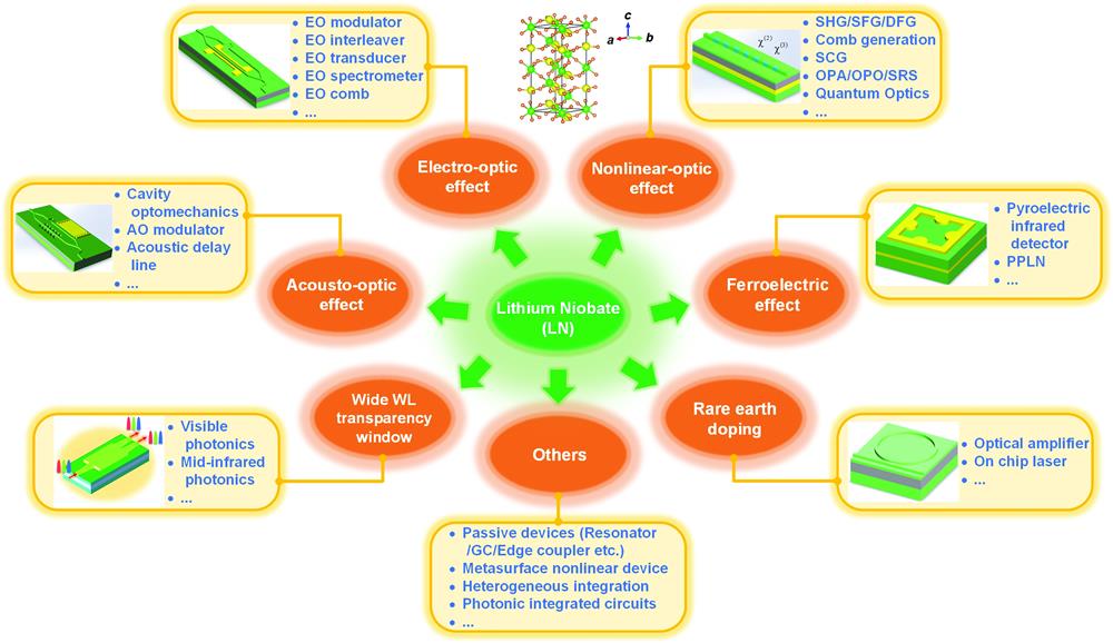
Figure 1.Overview of LN photonics. Top middle inset is LN crystal structure. EO, electro-optic; SHG, second harmonic generation; SFG/DFG, sum/difference frequency generation; SCG, supercontinuum generation; OPA/OPO, optical parametric amplification/oscillation; SRS, stimulated Raman scattering; PPLN, periodically poled lithium niobate; GC, grating coupler; WL, wavelength; AO, acousto-optic.
LN does not exist in the natural world and is a purely artificial inorganic material. It is composed of lithium, niobium, and oxygen. People usually refer to LN as a distorted perovskite type of crystal. In 1966, Bell Labs demonstrated single crystal LN and analyzed its material properties comprehensively.36–40 LN has a trigonal crystal structure (as shown in Fig. 1; top middle inset) and lacks inversion symmetry. There are many unique features of LN, such as a wide operational wavelength window, electro-optic (Pockels) effect, nonlinear optical polarizability, AO effect, rare earth doping possibility, pyroelectric effect, etc. These effects can be used for various applications, especially in photonics devices.
2.1 Basic Properties
LN is a birefringent crystal, and its ordinary () and extraordinary () refractive indices are 2.341 and 2.2547 at 500 nm wavelength,41 respectively. It has a wide wavelength transparency window, covering from the visible (400 nm) to the mid-infrared (),42 which makes it an attractive platform for many different applications. In the visible range, some applications, such as frequency metrology, quantum communication/computation, and light detection and ranging (LiDAR), can be realized based on the LN platform.42 While in the short infrared range, especially near 1550 nm which is important for telecommunications, LN has been widely used for light modulation based on both bulk LN and TFLN.31,43 For longer infrared wavelengths, some nonlinear optic conversions can be realized using LN.44 Ferroelectric LN has a large bandgap, which is calculated to be about 4.71 eV.45 A summary of LN material properties is shown in Table 1. Some details of these properties will be discussed in the remaining subsections and more details related to functional devices that exploit the various properties shown in Table 1 can be found in Sec. 4.
In an anisotropic material, the coefficients of the impermeability tensor , which change with increasing electric field strength, can be described by Eq. (1), where are known as the EO coefficients. As LN is a class 3m (ditrigonal-pyramidal) crystal, the EO coefficients can be described according to Eq. (2). The largest (-oriented) refractive index changes with respect to an applied (-oriented) voltage can be described by Eq. (3), where is the extraordinary refractive index and is the applied positive electrical field. As the relation between the refractive index change and the applied electrical field is linear, such an effect is also recognized as a linear EO effect or Pockels effect. By controlling the direction of the electric field, either an increase or a decrease in refractive index change can be obtained. For LN, () is most widely used for the design of EO devices,41 and this relatively high value is one of its main advantages. Many different kinds of modulators and EO tuning devices are reported based on such a property:31,52
2.3 Nonlinear Optic Properties
Another attractive property of LN is its high second- () and third-order () nonlinear susceptibilities. The second-order non-susceptibility of LN can be described by the two dimensional (2D) matrix shown in Eq. (4), where , , are the electric polarization components, , , are the electric field components, and are the second-order nonlinear susceptibility coefficients. For LN, typical values of , , and are 2.46, , and ,46 respectively. In addition, the third-order nonlinearity coefficient () of LN is estimated to be around .47 Both the high second- and third-order nonlinearities make LN an attractive platform for various kinds of applications, such as second harmonic generation (SHG),12,13,53–66 sum frequency generation (SFG),67,68 difference frequency generation (DFG),44 third harmonic generation (THG),62,69 optical parametric amplification/oscillation (OPA/OPO),70,71 stimulated Raman scattering (SRS),72,73 frequency comb,74–77 supercontinuum generation (SCG),64,78,79 and photon pair generation.80–83 Section 4 discusses these applications in detail.
2.4 Acousto-Optic Properties
When acoustic waves pass through a medium, they will cause elongation and local compression of the medium to produce elastic strain. The strain changes periodically with space and time, causing a medium to appear dense and then rare, just like a phase grating. Diffraction will appear when light passes through such a medium disturbed by acoustic waves, which is known as the AO effect (sometimes, it is also regarded as the photoelastic effect). The anisotropic AO relationship between the strain and the refractive index can be described by Eq. (5),2 where is a second rank tensor describing the refractive index change, is the second rank strain tensor, and is the fourth rank AO/photoelastic tensor. The detailed photoelastic coefficients of LN are shown in Table 1. The large photoelastic coefficients of LN together with its significant piezoelectric effect (for efficient acoustic waves launching) make multiphysics functional devices possible, such as AO modulators. Different from EO modulators, an AO modulator has bandpass frequency selectivity, which can complement low pass EO modulators:
2.5 Ferroelectric Properties
LN was reported to have ferroelectric properties as early as 1949,1 which means it exhibits spontaneous polarization characteristics with a nonzero electric dipole moment when there is no external electrical field. Such a property is commonly used for photonics application. For example, periodically inverting the crystal polarization direction of LN by applying a high electric field () to form periodically poled LN (PPLN) can be used for improving nonlinear conversion (examples are discussed in Sec. 4.3).80 For ferroelectric materials such as LN, the relationship between temperature variation and polarization intensity is usually described by the pyroelectric effect.2 In a pyroelectric crystal, varying the temperature will modify the positions of the atoms within the crystal structure; thus, its spontaneous material polarization will change correspondingly. Such a change in polarization state will result in a voltage rise across the crystal.2 If two surfaces (such as the top and bottom surfaces of Z-cut LN) of a crystal are covered with electrodes, there can be a current in the externally connected circuit. Such a current is proportional to the rate of temperature change and can be described by Eq. (6),84 where is the current, is the pyroelectric coefficient, is the surface area, and is the temperature change rate. For LN, was measured to be at 25°C.48 An intrinsically high pyroelectric coefficient in LN makes it a suitable platform for low cost and uncooled pyroelectrical photodetectors.
2.6 Thermo-Optic Properties
The thermal-optic (TO) coefficient of LN can be described by Eq. (7),50 where is the refractive index ( represents ordinary, represents extraordinary), is the temperature, is the wavelength, is the etalon length, is the temperature variation needed for complete detuning of the optical cavity, and is the thermal expansion of LN along the light propagation direction. Due to the birefringence property of LN, the thermal optical coefficient of LN is different for ordinary and extraordinary light. According to one measured result,50 the thermal optical coefficients of LN at around 337 K and 1523 nm are about and for ordinary and extraordinary light, respectively. The thermal conductivity of LN can be calculated according to Eq. (8), where is the thermal conductivity, is the density, is the specific heat, and is the thermal diffusion coefficient. The thermal conductivity of LN is also crystal orientation dependent. However, the difference is too small to distinguish. A typical value of thermal conductivity for either a- or c-oriented LN is around .49 Although these properties are not the highest among other materials, the TO effect in LN has still attracted some attention as it has a higher tuning efficiency and superior DC stability than the EO effect.85–87 Slower TO effect-based devices can be good complements to EO devices, especially in some areas where switching speed is not the primary consideration, such as in the case during calibration or tuning. One example is that the thermal tuning blocks can be used as phase shifters to control modulation bias points of an IQ modulator.88 For TFLN devices, the thermal tuning efficiency can also be improved by etching away underlying oxide.85,87 With the development of integrated LN photonics, TO-based devices will have more and more application scenarios.
2.7 Rare Earth Doping
Rare earth ions are solid state emitters with stable optical transitions with long lifetimes, making them good gain materials for optical amplification and lasers.89 In a typical fiber optic communication system, the silica fiber is doped with rare earth ions to form a fiber-optic amplifier/laser. Recently, rare earth doped integrated lasers, including different rare earth elements and laser cavity designs, have also been demonstrated on silicon photonics platforms.90 LN can also be doped with rare earth ions to realize interesting devices.91 With the development of TFLN technology, rare earth doped amplifiers92 and lasers93 have been demonstrated that can solve the chip-scale light source problem and pave the way toward large-scale photonic integrated circuits (PICs). The doping with these rare earth ions can take place either during the crystal growth phase94 or with postprocessing.95 More details about rare earth doped devices can be found in Sec. 4.5.
3 Processing Technology
3.1 Planar Device Technology
Light confinement is a fundamental problem in photonics applications generally. The refractive index of LN is around .41 Optical confinement and waveguiding require index contrast. In a typical planar bulk LN crystal, methods to introduce a refractive index contrast to form waveguides or other confinement structures can be divided into four main types:96 (1) Li-out diffusion, (2) metal ion-in diffusion, (3) PE, and (4) ion implantation. All of them form a planar device configuration.
3.1.1 Li-out diffusion
The Li-out diffusion method was first demonstrated by Kaminow and Carruthers.97 As LN can crystallize in a slightly nonstoichiometric form , its extraordinary index will increase linearly when the alloying variable decreases within a narrow range between 0.48 and 0.5. The change of can be realized by the Li-out diffusion of from the LN surface since the lithium ion has high mobility. Therefore, by applying a thermal treatment of an LN sample for several hours at high temperature, the refractive index will be changed in an LN target area as Li is diffused away.96 This method has two main disadvantages. One is that the refractive-index change occurs only in , and the other is that it is difficult to achieve selective diffusion.98 Therefore, although Li-out diffusion is proposed in principle and has been demonstrated in experiment,97,99,100 it is seldom used for photonics device fabrication. Alternatively, ion-in diffusion is more frequently adopted for LN device fabrication.19
3.1.2 Metal ion-in diffusion
During the metal ion-in diffusion process, a thin layer of metal is first evaporated onto an LN crystal surface, and then the crystal is heated at a temperature in a nonreactive atmosphere for several hours to make the metal diffuse into the crystal.19,98,101–112 A schematic of a photonic waveguide fabrication process based on ion-in diffusion is shown in Fig. 2(a). Different metals have been used for ion-in diffusion. Some of these are summarized in Table 2. The most widely used metal is titanium (Ti).19 The metal ion-in diffusion method is an easy and economical method for fabricating photonics devices. For experimental demonstration, as shown in Table 2, propagation loss below in photonics wires using such method has been realized.98,113–115 Before the appearance of TFLN devices, metal ion-in diffusion was widely used in photonic device fabrication. However, the refractive index difference formed by this method is very small (). Another method called PE can result in a slightly larger refractive index contrast,20,21 although also not very high overall.
Figure 2.Process flow of planar LN device fabrication. Illustration of (a) metal ion-in diffusion and (b) PE methods for planar photonic device fabrication in bulk LN crystals (dimensions are not drawn to scale). PR, photoresist.
In 1981, PE was first used to fabricate optical waveguides in LN.20,21 Different from metal ion-in diffusion, hydrogen ions are diffused into an LN crystal and are then exchanged with lithium ions during the PE process. The lithium ions then diffuse out of the crystal and finally the LN crystal is partially transformed into a new chemical with composition within a certain surface depth. The compound has several different phase states depending on the component proportion (), as validated by X-ray rocking curve analysis results and some other techniques.116 Several proton sources have been used for the PE process, such as benzoic, octanoic, adipic, glutaric, stearic acids, and their mixtures.117–119 Among them, benzoic acid is the most widely used proton source, as it has a high boiling point and stability throughout its liquid phase.116 A typical process flow for photonic device fabrication using PE is shown in Fig. 2(b). Compared with the metal ion-in diffusion method, the PE process has a much higher photorefractive damage threshold for visible light confining and transmission,120 as well as a higher resulting refractive index contrast.121 The PE process has been widely used to fabricate photonics devices in LN crystals with different orientations.116,121–126 Other than PE, a few other ions have also been used in such an exchange process with lithium to realize a refractive index change in LN.127–130 For example, Shah et al. demonstrated a kind of LN waveguide by immersing X-cut LN crystals in silver nitrate at 360°C temperature for several hours, and lithium/silver ion exchange was observed.127 Although with the more recent development of TFLN, direct dry etching has recently received more attention as it results in a much larger index contrast than either PE or ion-in diffusion, the PE method still has certain advantageous application scenarios, especially to assist dry/wet etching technologies to realize some innovative photonic devices.131
3.1.4 Ion implantation
Ion implantation can also be used for fabricating waveguides in LN crystals.132–137 Different from the above-mentioned methods, ion implantation results in a decrease of refractive index around the target area. Destefanis et al. implanted helium (He) ions into LN surfaces with about 1 to 2 MeV energies.132 They formed a low refractive index layer in the 2 to range just below the LN surface. Such a region of lower refractive index can form sufficient refractive index contrast for light confinement. It is worth mentioning that such a low index layer is very easy to etch by wet etchant, compared with these areas without damage. Therefore, such a buried layer can also be etched away to obtain a much larger refractive index difference.138 We will introduce this method again when we discuss wet etching. Other than the He ion, other ions have also been demonstrated for ion implantation of LN.133,135 Although a very large index difference can be obtained based on such methods, many more crystal defects will also be produced during the physical bombardment. Therefore, ion implantation has not been widely used for the formation of photonics devices in LN crystals. But He ion implantation is widely used in CIS technology, which is used for fabrication of TFLN. More details about TFLN process technologies are introduced in the subsequent sections.
3.2 Thin Film Lithium Niobate Fabrication Technology
Though bulk LN devices have been widely adopted during the past decades, their low index contrast and therefore weak light confinement have severely limited its further development toward large scale and dense integration. TFLN is thus proposed and developed to meet the advanced requirements of future devices. There are many different methods that have been proposed to create the TFLN. For example, TFLN can be directly sputtered onto a glass substrate,139 or grown on GaAs by pulsed laser deposition,140 or grown on a lithium tantalate substrate by the chemical vapor deposition (CVD) method.141 However, the directly grown/sputtering method may cause damage to the crystal quality as the measured EO properties are not as good as the bulk counterpart.139–141
3.2.1 Crystal ion slicing
In contrast, CIS technology can realize high-quality single crystal TFLN wafers and has widely been used since 1998.5,142–146Figure 3(a) shows a schematic of CIS technology. The processing starts from a bulk LN wafer, which is usually grown using the Czochralski method.147 Then, the bulk LN is implanted with He ions to a specific layer thickness (which depends on the desired TFLN thickness) to form a sacrificial layer. Helium (He) implantation is performed using an ordinary ion implanter. The He ion is the most widely used ion due to its small atomic mass.142 As the ion implantation will cause LN crystal damage that results in a different subsequent etch rate or thermal properties compared with undamaged areas, it can be comparatively easy to separate the top thin film layer from a bulk LN using a simple etching method, such as hydrofluoric acid (HF) etching. Then, the thin film layer is bonded to a bottom insulator layer using mature wafer bonding methods.9 Usually, the bottom insulator is selected to be a material with a lower refractive index, such as silicon oxide. The large resulting refractive index contrast between the LN and the bottom insulator enables strong light confinement within the LN layer. It is worth mentioning that the bottom substrate is not only restricted to LN, glass or Si is also possible. Furthermore, a thin layer of metal can also be inserted between the substrate and insulator layer to form a bottom metal electrode.
Figure 3.Process flows of (a) CIS and (b) lapping and polishing technologies. Dimensions are not drawn to scale.
In addition to CIS technology, the lapping and polishing method has also been developed for LN film fabrication. Figure 3(b) shows the process flow of the lapping and polishing method. The thick bulk LN wafer is first bonded onto a substrate with an insulator (of lower refractive index) inserted between them. Then, the top LN layer is thinned down to a few microns thickness by successive lapping and polishing.29,30 Compared with the CIS method, the LN film thickness after lapping and polishing is a little bit thick (typically around a few microns) and thus results in a larger device size. However, there are some advantages of LN films made by this technology. First, lapping and polishing is a purely mechanical process and thus has a smaller influence on crystal quality compared with CIS technology. In addition, the larger waveguide core in thick LN films enables a better coupling efficiency and a much higher laser-damaged threshold compared with thinner LN films.29,30,148–154 Therefore, lapping and polishing is a good complement to CIS technology.
3.3 Heterogeneous Integration
In the previous subsection, we introduced a kind of TFLN by wafer bonding a thin layer of LN onto an insulator with a lower refractive index (LNOI structure). In such a structure, 3D waveguides are directly etched to enable light transmission, and thus most of the optical field can be confined within the LN layer. There is another way to realize interaction of light with LN crystal, though, where the LN is not patterned at all. We refer to such a method as heterogeneous integration of LN with other material systems. As far back in 2009, Solmaz et al. demonstrated a type of integrated ring with Ti-diffused LN. As the refractive index of is very close to LN ( is 2.4, LN is 2.2), the transmitted light inside a Ti diffused LN waveguide can be vertically coupled into an waveguide.155 Since then, various kinds of heterogeneous integration schemes have been demonstrated, as summarized in Table 3.
Year
Cut
Structure
Thickness
Device
Integration method
Ref.
2009
X-cut
470 nm/N.A.
Ring
Magnetron sputtering
155
2011
Z-cut
Ring
Bonding
156
2012
Z-cut
Ring E-field sensor
Bonding
157
2013
Y-cut
Ring modulator
Bonding and deposition
158
2014
X-cut
a-Si:H/LN
90 nm/N.A.
MZI modulator
PECVD
159
2014
Z-cut
Ring modulator
Bonding
160
2015
N.A.
LN/silica
Whispering-gallery-mode resonator
Excimer laser ablation
161
2015
X-cut
MZI modulator
PECVD
162
2015
Z-cut
95 nm/600 nm/N.A.
Waveguide
Magnetron sputtering
163
2015
Y-cut
MZI modulator
Bonding and E-beam evaporation
164
2016
X-cut
PPLN waveguide
Magnetron sputtering
54
2016
Y -cut
MZI modulator
Bonding and PECVD
165
2017
X-cut
300 nm/850 nm/N.A.
Waveguide
LPCVD and Bonding
166
2017
X-cut
Si/LN
145 nm/N.A.
Resonator
Bonding
167
2019
X-cut
Photodetector
PECVD
34
2020
X-cut
MZI modulator
PECVD
168
2020
X-cut
MZI modulator
LPCVD
169
2020
X-cut
200 nm/225 nm/N.A.
MZI modulator
Bonding
170
2020
X-cut
200 nm/300 nm/N.A.
Spectrometer
PECVD
171
2020
Z-cut
Superconducting SPD
ALD
172
2020
N.A.
500 nm/400 nm/N.A.
Mode (de)multiplexer
Spin coating
35
Table 3. Summary of heterogeneous integration of LN with other material systems. ALD, atomic layer deposition; N.A., not available/applicable; a-Si, amorphous silicon.
These schemes can be divided into two categories. The first involves directly bonding/growing TFLN onto other mature material platforms,156,157,160,161,166,170 such as SOI wafers. Here, the light is confined inside these mature material layers with patterned structures, and the optical mode is designed to partially overlap with a top bonded/grown LN layer. Figures 4(a)–4(c) show an example of an LN on silica hybrid micro-resonator.161 About 15.47-nm root mean square (RMS) surface roughness is measured, which supports highly efficient EO application. The other scheme involves integrating or depositing a thin layer of a specific material (which is typically easier to dry etch than LN itself) that has a similar refractive index with LN above/onto the TFLN.34,35,54,155,158,159,162–165,167–169,171–174 Usually, these materials are directly grown on the LN surface, with a method such as magnetron sputtering,54,155,163 plasma-enhanced chemical vapor deposition (PECVD),34,159,162,168,171 or low-pressure chemical vapor deposition (LPCVD).166,169 As shown in Figs. 4(d) and 4(e), by patterning the deposited above the LN, the optical mode can be confined well inside the waveguide and an EO modulator can thus be realized.169 In such a scenario, the introduced material together with the LN layer forms the light confinement structure. Thus, the overlap of the optical mode and the LN layer is designed to be large. In addition, an etchless TFLN platform with photonic bound states in the continuum (BIC) has also been demonstrated recently through direct patterning of the above integrated organic polymer.35,173,174 In both methods, the LN layer is usually not patterned, and the geometry of the structure is defined in the other material with a more mature processing technology. Therefore, these methods avoid the well-known problem of LN crystals being difficult to etch.175 When there are no good etching solutions of LN available, heterogeneous integration becomes a good choice. Various types of devices have been realized based on these two schemes, as shown in Table 3. It is worth noting that the applications presented are not limited to active devices, as passive devices can also be realized. For example, hybrid grating couplers (GCs) for light coupling based on patterned Si176 and gold (Au)177 have been demonstrated. As the propagating optical field is only partially overlapping the LN crystal, the interactions between the light and LN are not maximized relative to what they would be if the light were instead fully confined within the LN. However, such methods are still attractive as they combine both the advantages of LN and the other well-developed material platform chosen, while avoiding difficulties associated with LN fabrication processes.
For both bulk LN and TFLN, there are strong motivations toward direct etching to form 3D structures.178 Dry etching is one of the main methods to realize such a goal. The plasma of a chemically active gas together with an inert ion plays the main roles during dry etching. As summarized in Table 4, many different kinds of dry etching methods have been demonstrated during the past decades. These demonstrations can be divided into three categories. One involves using the plasma of pure halogen ions,179,180,182,183,194,196 such as sulfur hexafluoride (), carbon tetrafluoride (), and boron trichloride (). As halogen ions will chemically react with the lithium, the reactant produced in the process of dry etching will be a problem and later affect device performance. Figures 5(a) and 5(b) show the scanning electron microscopy (SEM) image and current changed along the etching depth in end point detection after etching, which clearly shows the byproduct layer.182 Nagata et al. tried to remove the reactant using an additional wet etching method.179 The second category involves mixing the halogen ions with argon (Ar) in the plasma.178,182,185,186,188,189,191,193,195 Ar ion-based etching is a pure physical bombardment process. By engineering the gas flow ratio between the Ar and halogen element, the etch rate, profile, and surface conditions can be improved. In such a method, the halogen ions can still be a problem and affect the etching quality. Therefore, people have developed the third category of using pure Ar gas for etching.175,184,190,195 Compared with the first two methods, pure Ar-based etching has a lower etching rate, as the ion bombardment is a pure physical process. Its advantages are flat and clear surface condition, as evidenced by the SEM, AFM, and X-ray photoelectron spectroscopy (XPS) results shown in Figs. 5(c)–5(e).175 By using Ar-based etching, nearly vertical side walls52,175,197 and ultralow propagation loss197 have been observed; this method can then find wide use for photonics device fabrication. During such dry etching processes, a hard mask is typically used in addition to photoresist to improve the etching selectivity, as summarized in Table 4.
Year
Cut
Type
Etch gas
Resist
Mask
Etch rate
Selectivitya
Etch type
Ref.
1981
X-cut
Bulk
, Ar,
AZ 1350-J
Ni/Cr
55 nm/min
b
RIE
178
1998
Z-cut
Bulk
N.A.
Ni
N.A.
Plasma etching
179
2000
X-cut
Bulk
N.A.
c
N.A.
Plasma etching
180
2007
Z-cut
TFLN
Ar
SU-8
N.A.
N.A.
N.A.
Plasma etching
181
2008
X/Y/Z-cut
Bulk
, ,
N.A.
Ni/NiCr
2 to 3/10 to 53/37 to
3–10
RIE/ICP/ICP
182
2009
Y-cut
Bulk
TI09 XR
Ni
20 to 50 nm/min
20
RIE
183
2009
Z-cut
TFLN
Ar
OIR 907-17
N.A.
7.67 nm/minc
N.A.
ICP
184
2010
X-cut
Bulk
, Ar
AZ5214
Cr
97.5 nm/min
8.1–16
ICP
185
2010
X-cut
Bulk
, Ar
N.A.
Cr
92.5 nm/min
N.A.
ICP
186
2011
X-cut
Bulk
, , He
PMMA
Cr
280 nm/min
N.A.
ICP
187
2012
Z-cut
Bulk
, Ar
AZ5214E
Cr
98.6 nm/min
12
ICP
188
2015
Z-cut
Bulk
, Ar
N.A.
Ni
100 nm/min
7
ICP
189
2016
X-cut
TFLN
Ar
S1828
N.A.
12 nm/min
N.A.
ICP
190
2018
Z-cut
TFLN
, Ar
N.A.
Cr
N.A.
7
Plasma etching
191
2018
X-cut
TFLN
Ar
N.A.
N.A.
N.A.
N.A.
RIE
192
2019
Z-cut
TFLN
, , Ar
PMMA
0.69
RIE
193
2019
X-cut
TFLN
Ar
HSQ
N.A.
N.A.
N.A.
ICP
52
2019
Z-cut
Bulk
,
N.A.
Cr/Cu
812 nm/min
77
ICP
194
2021
X/Z-cut
TFLN
Ar
ma-N 1400
Cr
15 to 30 nm/min
1.4
ICP
175
2021
X-cut
TFLN
, Ar; , Ar; Ar
MMA/PMMA
Cr
35 to 50 nm/min; 20 to 33 nm/min; 12 to 18 nm/min;
N.A.
ICP
195
Table 4. Summary of LN dry etching technologies. PMMA, polymethyl methacrylate; HSQ, hydrogen silsesquioxane; MMA, methyl methacrylate; N.A., not available/applicable; RIE, reactive ion etching; ICP, inductively coupled plasma.
LN can also be etched by the wet etching method. Compared with dry etching, wet etching can realize a more uniform surface and much higher etch rates.198 In addition, wet etching is an economical and simple method compared with other etching technologies and is widely used in other material systems.109 It has been demonstrated that after the PE process, for instance, LN shows a larger etch rate using the mixture of HF and nitric acid (), compared with LN areas that are not subjected to the PE process.199 Therefore, the combination of PE and a mixture of HF and etchant is widely used for LN wet etching.109,199–204 Compared with dry etching, its etched sidewall is not too deep and there can be an underetching problem. Ting et al. demonstrated that the etching depth and aspect ratio can be improved using a diluted PE source with a lithium compound.198 By optimizing different molar percentages of adipic acid and lithium compounds, a very high aspect ratio [defined as etched depth divided by horizontal distance of the slant , as shown in Figs. 6(a)–6(f)] has been realized. Such an improvement can be clearly seen from the SEM images shown in Figs. 6(a)–6(f). The underetching problem can be alleviated by annealing (improve the adhesion of hard mask), as demonstrated by Hu et al.205 Some researchers also demonstrated that by adding some ethanol into the mixture, the etched surface of LN can be much smoother.205 PE is not the only way to cause a subsequent LN etching rate difference. Wang et al. found that and ion implanted regions can be etched more easily than those protected by a photoresist mask using a mixture of HF and at room temperature.206 Si et al. demonstrated that He ion implantation caused crystal damage in LN, which consequently also showed a higher chemical etching rate,138 and photonic crystal waveguides were successfully realized using such a method, as shown in Fig. 6(g). Using an ion beam enhanced etching method, a similar damaged layer can also be obtained.207 Copper (Cu) ion implantation with the assistance of HF solution has also been validated as a good way to achieve wet etching of LN crystals, and an etching rate of around has been observed.32 Up until now, most of the reported wet etching methods have been demonstrated in bulk LN crystals. But we believe wet etching is also suitable for TFLN devices, especially in some scenarios where cantilever structures are needed.
In addition to the above-mentioned methods, some other methods have also been used for the patterning/etching of LN. Most of them have been based on the physical polishing/milling process, such as focused ion beam (FIB) milling,208–211 dicing,212,213 femtosecond laser micromachining,214–218 and chemomechanical polish lithography (CMPL).214,215,217,219–223 FIB itself is a pure mechanical milling process, which either can be used along208,209,211 or together with other dry etching methods for layout patterning.208,210 For prototype validation, FIB is a good choice. But it will not be suitable for mass production of devices of any type due to economic and operability considerations. By contrast, dicing is an efficient method for quick fabrication of optical waveguides, as it can realize smooth sidewalls and a high aspect ratio.212,213 Recently, femtosecond laser ablation combined with FIB214–218 or CMPL214,215,217,219–221 has also been demonstrated for LN crystal patterning, which has received wide attention. Such a method can be divided into three steps. First, the LN crystal or metal mask is ablated with tightly focused femtosecond laser pulses, which is usually performed in water to reduce the possibility of debris and cracks.215 Second, the LN crystal is polished by the FIB or CMPL process. Third, the underlying oxide is partially etched using a wet etching method. Very high quality factor ( factor) () microresonators have been demonstrated based on such a method,224 which proves the very high quality of the etched sidewall. These mechanical milling methods together with the above introduced processing technologies pave the way for the fabrication of various LN photonics devices.
4 Functional Devices
Compared with other materials systems, LN has many unique features, such as large EO, NLO, and AO effects. The details of these effects are described in Sec. 2. For a long time, LN-based photonics devices were demonstrated only in bulk LN crystals, such as the Ti diffused EO modulator that is widely used in current fiber-optic communication systems due to its large bandwidth and superior linear EO response.3 The recently developed high-quality TFLN together with various etching technologies, however, has made significant headway toward integrated LN photonics. Many different kinds of photonics devices fabricated in bulk LN have now been demonstrated in TFLN, including passive devices, EO devices, nonlinear optical devices, AO devices, rare earth doping devices, pyroelectric devices, TO devices, etc.
In this section, we will give a review of functional devices demonstrated in LN during recent years. These devices cover both bulk LN and TFLN, which make use of the effects discussed in Sec. 2 and some key technologies demonstrated in Sec. 3. Here, bulk LN based devices are introduced for comparison with TFLN devices and will not be the main focus as they have been widely discussed in other reviews.2,3 From a comprehensive history of LN device evolution, we hope readers can be inspired to achieve improved designs of high-performance devices in the future and contribute to the further development of LN photonics generally.
4.1 Passive Devices
The waveguide is the most basic photonic device, as it confines light inside a specific region through refractive index contrast. As discussed in Sec. 2, there are many different ways to realize such a refractive index contrast. In a typical bulk LN crystal, ion-in diffusion, PE, and ion implantation are mostly used to define planar waveguides, while for TFLN, direct etching, including dry etching, wet etching, and a few other types of physical etching can be used to form waveguides for light confinement. Compared with ion-in diffused or PE bulk LN, the large refractive index contrast present at the interface of the top LN layer and the underlying bottom insulator in TFLN makes some compact and low loss devices possible. Researchers have developed several ways to characterize waveguide loss, such as cutback, sliding-prism, Fabry–Perot resonance, and scattered light methods.225,226 In addition, the propagation loss can also be extracted from the factor of a microresonator,42,192 which is inversely proportional to the factor of the microresonator.
4.1.1 Microresonator
In past years, various kinds of microresonators have been demonstrated both in bulk LN and TFLN platforms.43,181,192,193,197,214–218,221,222,224,227–240 In bulk periodically poled Z-cut LN crystals, a high factor of was measured by mechanically polishing the LN crystal,227 as shown in Fig. 7(a). The factor of the TFLN-based microresonator is increased gradually. In 2014, Wang et al. demonstrated a kind of microdisk in TFLN using Ar-based electron-cyclotron resonance (ECR) reactive ion etching (RIE), and its measured factor was around [Fig. 7(b)].228 This was just at the early stage of TFLN devices. Such a value can be further improved by optimizing design and processing technologies. For example, a microring with a factor up to was demonstrated in 2017 using an optimized Ar-based dry etching process, which corresponds to a propagation loss as low as .192 An SEM image of this kind of etched microring and its corresponding measured transmission spectrum are shown in Figs. 7(c) and 7(d), respectively. These results validate the fact that Ar-based etching is a suitable method for TFLN patterning. Meanwhile, many other groups have also demonstrated high factor based on such a method.197,230,231,234,236,237 More recently, a record-high factor up to (calibrated by considering transmission rates of modes) at 1550 nm wavelength was achieved using the femtosecond laser-assisted CMPL method224 [as shown in Figs. 7(e) and 7(h)], which indicates a propagation loss of around . Such a result is realized using a pure mechanical polishing process, thus avoiding the possible ion-induced lattice damage. This ultralow loss device opens up many prospects toward broad application of LN photonics, especially for various nonlinear applications. Compared with bulk LN devices, low loss or high factors are not the main advantages of TFLN-based microresonator, however, as ultrahigh factors have also been demonstrated in bulk LN devices.227 More advantageous is the fact that the larger refractive index contrast in TFLN enables various microresonator forms that are ordinarily extremely difficult or impossible to realize in bulk LN. Here, our discussion on microresonators is limited to microrings or microdisks. Actually, some other types of microresonators have also been demonstrated in LN (mainly TFLN), such as photonics crystal (PhC)241 and distributed Bragg reflector (DBR)-based Fabry–Perot (DBR-FP)242,243 resonators. Recent progress of EO modulators based on PhC and Fabry–Perot microresonators is discussed in Sec. 4.2.1.
Due to the strong mode confinement in TFLN, many other passive blocks have subsequently been demonstrated.85,131,176,177,223,244–269 The fiber to chip interface is a basic function as it determines how much light can be coupled into a photonic device. There are two types of methods to couple the external light into a chip. One is vertical coupling of light onto a chip using a GC.176,177,245,247,248,252,254,259,265,266,268,269 The other is based on edge coupling,223,246,249,258 which couples light into a chip horizontally. According to the operation principle, GCs can also be divided into two categories, one is the one-dimensional (1D) GC and the other is the 2D GC, both of which have been demonstrated in the LN platform. For a 1D GC, the design strategy is to optimize the periodic structure to realize the phase matching condition for best coupling efficiency. A high coupling efficiency of () has been realized in Z-cut TFLN with a bottom Au reflector, and the grating has been designed with a chirped structure to improve its coupling efficiency,259 as shown in Figs. 8(a)–8(c). The typical coupling efficiency of a 1D GC is between and .176,177,245,247,248,252,254,268,269 A 2D GC is more functional as it can realize the demultiplexing of orthogonal polarization multiplexed signals while coupling light into on-chip devices.270 Although there are many reports about 2D GC in other material systems, similar research is very limited in TFLN. Chen et al. demonstrated a kind of 2D GC in TFLN with measured coupling efficiencies of at 1561 nm for P-polarized light and at 1568 nm for S-polarized light,265 as shown in Figs. 8(d)–8(f). Their measured 1-dB bandwidths for both P- and S-polarized lights are around 30 nm. Such demonstrated results are far from comparable to those of its counterparts and hence need more efforts to improve. Both 1D and 2D GCs allow for wafer scale on-chip testing without the need of chip dicing. GCs are more difficult to realize in bulk LN compared with TFLN due to its smaller refractive index contrast.
Compared with the vertical GC, an edge coupler is less sensitive to polarization, has a larger operating bandwidth, and enables lower insertion loss. Its main drawbacks are that accurate facet polishing and sample dicing are needed. For edge coupling, the main optical loss mechanism is the mode mismatch between the fiber and on-chip waveguide. Therefore, design strategies are to tailor both the fiber and waveguide modes to reduce the mode mismatch and thus improve the coupling efficiency. By adiabatically tapering a standard single-mode fiber to match a specially designed LN waveguide, Yao et al. demonstrated a measured coupling efficiency for transverse electric (TE)/magnetic (TM) modes.223 Using a monolithic bilayer mode size converter, He et al. also demonstrated a measured coupling loss,246 as shown in Figs. 9(a)–9(c). By combining a silicon oxynitride cladding waveguide with the bilayer LN taper, the coupling efficiency is further reduced to per facet at 1550 nm for TE/TM light.266 A multiple layer mode size converter shows a possible solution for low loss edge coupling in TFLN. Compared with the SOI platform, the refractive index contrast in TFLN is smaller and thus results in weaker mode confinement and larger waveguide bending radii. However, a comparable low coupling loss can also be obtained in TFLN by reducing the mode size mismatch between the fiber and waveguide. We believe there is still room for performance enhancement of edge coupling in the LN platform, as lower coupling loss () has already been demonstrated in ion-in diffused bulk LN devices.271
In addition, mode-related devices,131,244,250,251,255,261,262,267 TO-based devices,85–87 Bragg grating filters,253,256,257,264 optical true delay lines,263 and optical phased arrays260 have also been demonstrated in the LN platform. Most of them rely on the large refractive index contrast available in TFLN. Similar to its counterpart, which is SOI, these passive blocks can be combined together to form more powerful chip scale PICs. And researchers have already tried to do so. For example, a two-mode (de)multiplexer is realized by combining a passive Mach–Zehnder interferometer (MZI) and an EO tuning electrode.131 This will be a trend as PICs can solve power consumption and device size problems that are inherent in conventional bulk LN devices.
4.2 EO devices
4.2.1 Electro-optic modulator
Compared with other material systems, the most attractive feature of LN is its large EO coefficient, which can be used for fabricating high-performance modulators. Different from the plasma dispersion effect-based modulators in silicon photonics10 and the electro-absorption-based modulators in III–V platforms,11 there is no carrier dynamic process in LN-based modulators where the speed is mainly limited by the microwave electrode. Therefore, Pockels effect-based linear LN modulators can achieve higher modulation speeds.31,52 Therefore, LN-based modulators are widely used in current fiber-optical communication systems. For a long time, these modulators have been fabricated in bulk LN crystals using the technologies described in Sec. 2. For example, a Ti-diffused ring resonator in a bulk LN crystal can achieve around a tuning efficiency.43 However, these bulky devices have a large device size and cannot meet the requirements of dense integration in current/future large capacity optical interconnect systems. The TFLN platform is well poised to solve these problems. In the same year, Guarino et al. demonstrated an EO tunable microring resonator in TFLN using CIS and wafer bonding technology.181 Its structure is shown in Fig. 10(a), where the Z-cut TFLN is directly etched and inserted between the top and bottom electrodes. As shown in Fig. 10(b), the measured tuning efficiency is about from the observed wavelength shift.181 Such a value is lower than results demonstrated in bulk LN, which is probably due to the lower electric field strength inside the waveguide and can perhaps be improved by changing the design. Subsequently, with the high-quality TFLN that is now commercially available, various kinds of modulators have been demonstrated.31,52,88,241–243,272–288 Some of the reported modulators in LN platforms are summarized in Table 5.
In terms of device configuration, there are some structures such as microrings,272,292 MZIs,31,52,88,272,274,275,277,278,281–285,287 Michelson interferometers,273,276,279 PhC cavities,241 and DBR-FP modulators,242,243 as shown in Table 5 and Fig. 11. Different configurations have different advantages. For example, microring-based modulators have compact sizes,272,292 and Michelson interferometer modulators (MIMs) [Fig. 11(f)] can realize reduced half-wave voltage-length product () due to doubled interaction between the light wave and electric field compared with MZI structures.273,276,279 The improved tuning efficiency of PhC-based [Figs. 11(d) and 11(e)] and DBR-FP-based [Figs. 11(g)–11(i)] modulators is based on a similar principle.241–243
In most reported results, the amplitude of the input light is modulated by an applied electrical signal (amplitude modulation). As shown in Figs. 11(a)–11(c), around nonreturn to zero (NRZ) and up to 8-ASK (8 level amplitude modulation) are measured using an optimized MZI TFLN modulator. For a 20-mm long arm length, its measured (defined as the forward transmission coefficient from port 1 as input to port 2 as output when port 2 is matched for a two-port network and was widely used to characterize the speed of optoelectronic devices) is above 40 GHz. The authors also demonstrated that its can be improved up to above 80 GHz by reducing the arm length.31 Some other modulation dimensions can also be added into the TFLN modulator.88,294 In 2020, Xu et al. first introduced the phase modulation dimension into a TFLN modulator and realized transmission speeds up to based on the 16 quadrature amplitude modulation (QAM) format.88 More recently, researchers from the same group further demonstrated a TFLN-based dual-polarization in-phase (DP-IQ) modulator with record data rate.294Figures 11(j) and 11(k) show a schematic of the DP-IQ modulator with a 2.35-cm long arm and its corresponding measured curves. The researchers used double polarizations and a quadrature amplitude phase modulation format. For each single MZM, the measured is above 110 GHz under 1 V voltage. Such a high bandwidth enables 400-QAM and thus realized a record total data capacity. By engineering the electrode transmission line282,295 or introducing more multiplexing dimensions, such as mode division multiplexing,24 the transmission speed/volume can be further improved.
In addition to speed, some other key metrics are also critical to evaluating modulator performance, such as , as well as insertion loss (IL). As shown in Table 5, most reported results have an average between 1 and .52,88,272,273,276–280,282–285,287 Using a dual-capacitor electrode layout, the can be reduced to as low as .281 Such a factor is highly related to the device structure and can likely be improved by optimizing the design. The overall low values of LN-based modulators are highly desirable for their application scenarios.
It can be observed from Table 5 that most of the reported LN-based modulators have low IL (excluding coupling loss),31,52,88,241–243,272,275,277,282,287 which depends on the device dimension and fabrication technology. A typical bulk LN-based modulator is usually fabricated using ion-in diffusion technology. For TFLN modulators, Ar plasma-based dry etching is widely used to pattern the LN waveguide structures, which can realize a low propagation loss (also depends on etching conditions) compared with bulk devices. By optimizing the processing technology, the TFLN waveguide with a more prevailing propagation loss of lower than can be obtained.31 Thus, high-performance LN-based modulators with lower IL can be expected in the future.
Extinction ratio (ER) is another metric to characterize a modulator’s performance. In most published LN-related results, ER is defined by the valley value [such as the minimum value shown in Fig. 10(b)] of the transmission spectrum.181 A high ER gives a better modulation signal quality, such as more open eye diagrams during data transmission experiments. The typical ER in literature is between 10 and 30 dB,282,285,292 which can be improved by optimizing either process technology or design. Take the MZI as an example, and usually the Y-branch is used as the power splitter. However, if the optical power difference between the two arms is too large due to the imperfect fabrication process technology, its ER will be degraded. By optimizing the fabrication process, or changing the Y-branch structure with a multimode interferometer (MMI, more tolerant to fabrication process error compared with Y-branch),296 a higher ER can be realized. In addition, using cascaded MZI274 or Bragg grating waveguide,243 ultrahigh ERs have been demonstrated, which are other examples of improving ER by optimizing design.
In summary, there are many different criteria to evaluate a modulator’s performance. Although there are many different kinds of LN-based modulators that have been demonstrated, none of them can realize all the best metrics at the same time. The tradeoffs exist, thus there are still optimizing spaces for the research community.
4.2.2 Other electro-optic devices
The superior EO effect of LN is not only limited to the modulator application, as it can also be extended to various other kinds of application scenarios. One of the key benefits that may result from the development of TFLN is that a variety of different components can be integrated on the same chip to enable more functionality overall. The physics behind them is generally the same as EO modulators, which is by changing the material refractive index and thus the phase. Some typical EO-based applications demonstrated on TFLN platform have been summarized here.
First, the fast EO tuning features can be used in optical fiber communication or optical interconnects. For example, Fig. 12(a) shows EO tunable interleavers,297 which can be used as tunable filters or wavelength-selective switches. Their measured tuning sensitivity is [Fig. 12(b)] and [Fig. 12(c)] for TE and TM modes, respectively. Compared with TO-based tuning, EO tuning enables a much higher speed and thus has broader application perspectives.
Second, the EO effect of LN can also be used for controlling the optical frequency, which enables broad applications, such as advanced photonic computation and frequency-domain photonic quantum computers.298,299Figure 13(a) shows an example of a programmable photonic two-level system for controlling gigahertz microwave signals, and its working principle is shown in Fig. 13(b).298 Benefits from the low loss TFLN ring resonator and cointegrated microwave electrode, the authors have demonstrated electrical bandwidth, around modulation efficiency, and photon lifetime.298Figures 13(c)–13(e) show another example of an on-chip EO frequency shifter for frequency controlling using only a single-tone microwave signal.299 In that work, the authors have realized frequency shifts as high as 28 GHz with an approximately 90% on-chip conversion efficiency (CE) and shift ratio (defined as the ratio of the output power at the shifted frequency and the output power inside the bus waveguide). Both works pave the way of efficiently and precisely manipulating light on gigahertz frequency, and open doors to many application scenarios.
Third, an LN-based microwave to optical transducer for quantum networks is another application scenario, especially under the conditions of rapidly developed quantum computation and long-haul quantum communication systems.300–302 The typical microwave to optical conversion is based on electro-optomechanics (EOM) in a bulk optical cavity, which is difficult to operate at the quantum ground state as the mechanical cavity has a limited frequency.302,303 An LN with the large Pockels effect enables GHz microwave to optical photons conversion and thus attracts significant attention. Holzgrafe et al. used the EO effect in coupled TFLN microrings, realizing an efficient microwave-to-optical transducer [Fig. 14(a)].300 Its measured on-chip transduction efficiency is up to [Fig. 14(b)], which can be used to link up superconducting quantum devices with optical fibers. McKenna et al. demonstrated a similar microwave-to-optical transducer,301 and the TFLN sits on a sapphire platform. Its device structure is shown in Fig. 14(c), which consists of triple resonators. According to the measured results shown in Fig. 14(d), such a device converts microwave photons to optical photons with an on-chip efficiency of around . More recently, Xu et al. demonstrated an improved CE up to 1.02% in coupled ring resonators,302 as shown in Figs. 14(e) and 14(f). Such an improvement is realized using an air-cladding structure to mitigate the prominent photorefractive (PR) effect, which is supposed to be the main limiting factor of CE.302 Even though the highest CE in TFLN is still under expectation considering its high Pockels effects, we believe the gap between a typical EOM-based scheme (highest CE of 47%303) and a TFLN-based EO structure [currently of 300 or 301] can be further narrowed down by optimizing the design and fabrication technology. TFLN-based integrated transducers will play a significant role in future quantum networks.
The last example is a dynamic integrated Fourier-transform spectroscopy based heterogeneously integrated SiN on LN hybrid structure (detail about such integration technology can be found in Sec. 3.3), and its device details are shown in Fig. 15,171 where the EO properties of TFLN have been exploited for retrieving a complete spatial interferogram. This prototype device is capable of completely sampling the standing waves from signals over a 500-nm bandwidth. Using such a device, the authors have demonstrated a measured interferogram for a broadband optical signal from a super-luminescent light emitting diode, which has a 1550 nm center wavelength and a 50 nm 3 dB bandwidth. The above-discussed results are just a few examples based on the EO effect of LN for extended applications. We believe the applications are not limited to these and more advanced devices/PICs will be demonstrated in the future.
LN is also an excellent platform for various nonlinear and quantum photonic applications due to its significant nonlinear effects. In typical bulk LN, nonlinear applications are mainly limited to areas of frequency conversion. For TFLN, on the other hand, due to the convenience of dispersion engineering, some applications such as optical frequency comb and supercontinuum generations typically demonstrated on silicon photonics platforms can also be realized with superior performance contributed by its improved confinement and better overlap with light.
The nonlinear dynamics in both bulk LN and TFLN need to satisfy the phase-matching condition for conservation of momentum, which can be achieved using birefringent phase matching.80 Such a method is difficult to realize in both bulk LN and TFLN waveguide structures and has lots of challenges, such as low effective nonlinear effects and inconvenient phase-matching temperatures and angles.304 An alternative method is called quasiphase matching (QPM) and can be realized by periodically inverting (poling) LN ferroelectric domains to point alternatively to the +c and −c directions to form PPLN.80 Compared with bulk LN, an advantage of TFLN structures is their flexibility in dispersion engineering by varying the waveguide dimension,55,79 which provides an additional degree of freedom for fine-tuning the phase-matching condition.
LN-based devices for nonlinear and quantum photonic applications are summarized in Table 6. One of the main categories is frequency conversion, which can be realized either by frequency upconversion with SHG,12,13,54–56,58–61,63,65,66 SFG,67,68 and THG62,69 or by frequency downconversion with DFG.44 In bulk LN-based devices, their bending loss is typically large due to the small refractive index contrast available, and thus results in a large device size and also degrades the interaction between the light and nonlinear medium. For example, the CE of SHG in bulk PPLN is usually at the level of .12 In contrast, a nanophotonic thin film periodically poled lithium niobate (TFPPLN) waveguide can have CE as high as .58 Assisted by a high- cavity, a high CE of 250,000%/W SHG has been demonstrated in a periodically poled TFLN microring,63 as shown in Figs. 16(a)–16(c). Such a record ultrahigh CE is achievable from the ultralow loss/ultrahigh factor () microring resonator fabricated on a TFLN wafer with a large refractive index contrast. With future development of LN patterning and etching technologies, as well as material quality, an even higher CE can be expected on LN platforms. For example, as discussed in Sec. 4.1.1, the Q factor can be improved up to around using an optimized patterning technology,224 which would enable a greater nonlinear interaction of the optical field with the LN crystal. In addition, metasurface structures can also be used to improve nonlinear conversion in TFLN.306 Some experimental results will be summarized and introduced in Sec. 4.6.2. It is worth mentioning that devices in thicker (several micron-thick) LN films have some advantages in high-power frequency conversion, such as watt-level frequency generation, as they exhibit a higher power damaging threshold compared with submicron film-based devices. As shown in Table 6, around 1 W of second harmonic can be generated in a thicker LN film,153,154 using the lapping and polishing method (details in Sec. 3.2.2). The larger waveguide core also enables high global efficiency (considering insertion loss) due to its larger mode profile.29,30,148–154
Year
Cut
Type
Application
Performance
Fabrication
Ref.
1993
Z-cut
Bulk PPLN WG
SHG
CE:
PE and electrical poling
12
1996
Z-MgLN
Bulk PPLN WG
SHG
CE: a
Wet etching and electrical poling
13
2002
N.A.
Bulk PPLN WG
Photon-pair
CE:
PE and electrical poling
80
2004
N.A.
Bulk PPLN WG
SFG
CE:
PE
67
2006
Z-ZnLN
TFPPLN ridge
SHG
CE:
Lapping and polishing, dicing
29
2009
Z-MgLN
Bulk PPLN disk
THG
CE:
Mechanical polishing
69
2010
Z-ZnOLN
TFPPLN ridge
SHG
CE: 2400%/W
Lapping and polishing, dry etching
30
2016
Y-MgLN
TFPPLN ridge
SHG
CE: ;
Lapping and polishing
152
output power: 0.86 W
2016
X-cut
TFPPLN WG
SHG
CE:
HI and electrical poling
54
2016
ZnLN
TFPPLN ridge
Photon-pair
Rate: ;
Lapping and polishing
149
efficiency: 64.1%
2016
Z-cut
TFPPLN ridge
SHG
CE: 204%/W
Lapping and polishing, dicing
148
2017
Z-MgLN
TFPPLN
SFG
CE: 3.3%/W; BW: 15.5 nm
HI and bonding
305
2017
X-cut
TFLN WG
SHG
CE: ;
Ar ICP-RIE
55
phase matching free
2017
X-cut
TFLN WG
SHG
CE:
Ar ICP-RIE
56
2018
N.A.
TFPPLN ridge
Comb
Mid-infrared span
Lapping and polishing
150
2018
X-MgLN
TFPPLN WG
SHG
CE:
Ar ICP-RIE and electrical poling
58
2019
X-cut
TFLN WG
SHG
CE:
HI
59
2019
X-MgLN
TFPPLN ring
SHG
CE: 230,000%/W
Ion-milling and electrical poling
60
2019
X-cut
TFLN WG
SHG
CE:
Ion-milling and electrical poling
61
2019
X-cut
TFLN disk
SHG; THG
SHG: 9.9%/mW; THG:
Femtosecond-laser ablation and FIB polishing
62
2019
Z-cut
TFPPLN ring
SHG
CE: 250,000%/W
Ar etching and electrical poling
63
2019
Z-cut
TFLN WG
SCG
Span: 1.5 octaves
Ar ICP
78
2019
Z-cut
TFPPLN ridge
SFG
CE: 85%/W
Lapping and polishing, dicing
151
2019
X-cut
TFLN PIC
Comb
Comb generation and modulation (PIC)
Ar ICP-RIE
76
2019
X-cut
TFLN WG
SCG
Span: 2.58 octaves
Ar ICP-RIE
79
2019
X-cut
TFLN ring
Comb
Span: >80 nm
Ar ICP-RIE
77
2019
MgLN
TFPPLN ridge
SHG
CE: ; output power: 1.1 W
Lapping and polishing, dicing
154
2020
N.A.
TFLN disk
SHG
CE: (282.7 nm)
Simulation
306
2020
Z-cut
TFPPLN ring
Photon-pair
PGR: 36.3 MHz; CAR: >100
Ion-milling and electrical poling
81
2020
X-cut
TFLN WG
SHG
CE:
ICP and electrical poling
65
2020
Z-cut
TFLN disk
SFG
CE:
FIB and wet etching
68
2020
X-cut
TFLN ring
SRS
Pump-to-Stokes CE: 46%
Ar ICP-RIE
73
2020
X-MgLN
TFPPLN WG
Photon-pair
PCR: 11.4 MHz; CAR: 668
Electrical poling
82
2021
X-MgLN
TFPPLN WG
OPA
Amplification: >
Ar etching and electrical poling
70
2021
Z-cut
TFPPLN ring
OPO
Threshold: ; CE: 11%
Ar ICP-RIE and electrical poling
71
2021
Z-cut
TFPPLN ridge
SHG
CE: ; output power: 1 W
Lapping and polishing, dicing
153
2021
X-MgLN
TFPPLN WG
DFG
CE:
Ar etching and electrical poling
44
2021
X-cut
TFPPLN WG
SHG
CE:
ICP and electrical poling
66
2021
X-cut
TFPPLN WG
Photon-pair
Rate: ; SHG:
ICP and electrical poling
83
Table 6. Summary of LN-based devices for nonlinear and quantum photonic applications. MgLN, MgO-doped lithium niobate; ZnLN, Zn-doped lithium niobate; ZnOLN, ZnO-doped lithium niobate; PE, proton exchange; HI, heterogeneous integration; PIC, photonic integrated circuit; N.A., not available/applicable.
The optical frequency comb with periodic optical frequency lines has also been demonstrated in the TFLN platform77 while it is typically difficult to realize in bulk LN. Based on a dispersion-engineered microring with a high factor, Kerr comb generation has been demonstrated in the TFLN platform.63,74,75Figure 16(d) shows one example of an on-chip photonic integrated circuit (PIC) containing both Kerr comb generation and filtering.76 The microresonator frequency comb generator is based on the third order () nonlinear effect, while the add-drop filter is based on the second-order () EO effect. Its generated comb has a line spacing of , and spans of and for TM and TE modes, respectively. Compared with a third-order nonlinearity-based comb, an EO phase modulation-based comb features high stability and controllability, which has also been demonstrated in the TFLN platform.77 Such an EO comb is based on ring modulators and has over 80 nm bandwidth and more than 900 comb lines with a slope of , as shown in Fig. 16(e). Both the Kerr and EO combs show that TFLN is an excellent platform for comb generation.
TFLN can also be used for supercontinuum generation based on its second- and third-order nonlinear effects. Figure 16(f) shows an example of a supercontinuum spanning 2.58 octaves using dispersion-engineered TFLN waveguides. Its performance is highly related to the waveguide geometries. Benefiting from its large refractive index contrast, dispersion engineering becomes easy and more demonstrations on comb and supercontinuum generations can thus be expected.
Based on the strong second-order nonlinearity in TFLN, a broadband OPA70 and an ultralow threshold OPO71 have also been realized in dispersion-engineered TFLN devices. Figure 16(g) shows the principle of OPA in dispersion-engineered periodically poled TFLN waveguides. The general idea is to do engineering on the waveguide for low group velocity dispersion and group velocity mismatch, and thus maximize OPA performance.70 According to the measured results, broadband phase-sensitive amplification is larger than for a 2.5-mm long waveguide with pump pulse energy of only 0.8 pJ. Such a result paves the way for chip-based light sources.70 Raman scattering is another important nonlinearity and has been widely explored in other materials systems. Yu et al. demonstrated multiwavelength Raman lasing in a TFLN microring and analyzed the underlying physical process,73 which provides guidance for TFLN-based SRS dynamics.
In addition to the above classical applications, LN is ideally suited for quantum applications based on its large nonlinearity, such as photon pair generation.15,80–83,149 Although bulk LN has been used for quantum applications for a long time, the recently developed TFLN makes integrated and higher-efficiency devices possible. Figures 16(h)–16(j) show an example of a quantum photon source based on a TFLN microring.81 Its measured photon pair generation rate (PGR) is around 36.3 MHz using pump power, while its measured coincidence to accidental ratio (CAR) is above 100 at high rates and reaches at a low pump power. Both of these values are much higher than previous reported results, and such benefits mainly come from having highly confined TFLN devices together with the superior nonlinear effect. In general, with the development of recent advances in the TFLN platform, advantages of LN with its large and are increasingly being exploited. It is believed that many new phenomena and applications will be demonstrated based on the unique nonlinear properties of LN and will further contribute to the development of quantum photonic devices.
4.4 AO Devices
LN is also an ideal platform for the demonstration of AO devices due to its large photo-elastic constant,2 as such devices can be used in the area of optical networking and signal processing.16 For a long time, surface acoustic wave (SAW) derived AO devices have been extensively explored in bulk LN in combination with Ti diffusion/PE technology.307 Due to the weak mode confinement caused by the poor refractive index contrast available with those technologies, the interaction between the transmitted light and acoustic waves is not as high as desired. The recently developed TFLN platform provides an attractive choice for integrated AO devices. In 2010, Kadota et al. realized a high-frequency (4.5 and 6.3 GHz) Lamb wave resonator using direct -axis TFLN by the CVD method,308 which validates TFLN’s advantages for AO devices. In this part, we will focus on the latest results about TFLN-based AO devices. Selected bulk LN-based results will also be covered for comparison.
4.4.1 Cavity optomechanics
Benefiting from commercially available high-quality TFLN and well-developed LN etching technologies, high factor and small phonon mode size SAW resonators at gigahertz frequencies have been demonstrated by the engineering of photonic band structures,197,309–311 something that is inapplicable in the typical bulk LN platform. Figure 17(a) shows an SAW resonator based on chirping a quasi-1D PhC period, and its measured factor is 6240 at a fundamental mode frequency of 3.07 GHz [Fig. 17(b)], which results in an product of .311 In another optimized PhC structure, as shown in Figs. 17(c)–17(e), a mechanical mode frequency close to 2 GHz with a factor of around 17,000 at 4 K was obtained, which corresponds to around .310 These demonstrated high product optomechanics resonators pave the way toward hybrid quantum systems, enabling the control of solid-state electronic spins, AO modulators, gigahertz frequency optical comb generation, and performing microwave to optical conversion.17,311
AO modulators have already been demonstrated in LN platforms.16,17,312,313 Different from high speed EO modulators, AO modulators can be enhanced by a mechanical quality factor with bandpass frequency selectivity and also have no critical requirement of placing interdigitated transducers (IDTs) close to the optical waveguide, since acoustic waves have a low propagation loss.312 Thus, AO modulators can be a good complement to existing EO modulators.
Surface elastic waves can be generated by mechanical coupling of a shear or compressional wave transducer.314 However, for better interaction between acoustic and optical waves, the IDT structure is more frequently used.314Figure 18(a) shows a typical straight IDT structure, which consists of spatially periodic electrodes. Its key metrics involve the finger length (), finger number (), and finger period (). Based on the angular spectrum of plane wave theory, the amplitude field of the IDT can be calculated.315 To further improve the acoustic–photonic interaction, a concentric IDT is proposed, as shown in Fig. 18(b). In such a structure, the interdigitated electrodes are designed with circular arc shapes and hence can achieve higher intensity acoustic fields.315,316
AO devices have been demonstrated in bulk LN platform. In 1992, Cheng et al. demonstrated an AO frequency shifter with a measured 121 MHz tunable bandwidth (center frequency is 0 MHz) in the visible band based on Y-cut bulk LN.317 Passive waveguides are formed through Ti diffusion; thus, the device volume is typically in the cubic centimeter range. Kakio et al. demonstrated an AO modulator in a 128-deg rotated Y-cut LN crystal. Under a 17 V and 195 MHz driving voltage, about 84% diffractive efficiency was obtained.318 Similarly, such a device is based on a Ti diffused waveguide and thus presents a large device size (with an IDT length of 2 or 3 mm). In addition, due to the large device size in bulk LN, the modulation frequency is typically limited to several hundreds of megahertz. The TFLN platform can compensate for these drawbacks and thus realize more compact and efficient AO devices.312,313,319,320
Figures 19(a)–19(c) show both MZI and microring-based AO modulators in a TFLN platform, which uses IDTs for launching the SAW to reduce reflection losses.16 The photoelastic coefficient was extracted to be 0.053 from experimental data, which agrees well with the theoretical value. Based on the acoustic optic resonator/modulator, high-performance microwave to optical conversion has been demonstrated in TFLN.17 As shown in Figs. 19(d) and 19(e), in a suspended IDT-coupled TFLN MZI AO resonator, enhanced microwave to optical conversion at 2.24 and 3.33 GHz acoustic resonance modes is observed. From such an experimental result, the is estimated to be around 4.6 V, and is around (acoustic resonator length is ). It is known that the introduction of a resonant acoustic cavity will degrade the bandwidth of an AO modulator, and Hassanien et al. demonstrated a wideband (140 MHz) operation AO modulator without using any acoustic cavity.312 Its principle is shown in Fig. 19(f), which consists of a PhC waveguide for light confinement, and a split IDT designed to generate mode Lamb waves. Such a device is power efficient, with phase shifts up to over a modulation length, and its measured bandwidth is up to 140 MHz under a 1.9 GHz center frequency [Fig. 19(g)]. More recently, photonics BIC has also been demonstrated to realize high-performance AO modulation.319,320 As discussed in Sec. 3.3, BIC structures can realize low loss light transmission without the need for etching of TFLN and thus enable various integrated devices/circuits. Figure 19(h) shows an example of GHz AO modulation based on a photonics BIC waveguide.320 Compared with a typical bulk LN device, the improved modulation frequency is a consequence of the reduced device size and enhanced acoustic-photonics interaction.
In addition, TFLN is also suitable for the fabrication of an acoustic delay line (ADL) that can be used for radio frequency (RF) acoustic signal processing.321 By choosing the fundamental symmetrical () mode, low IL and large fractional bandwidth (FBW) at a high frequency can be realized,321–323 which overcomes the drawback of fundamental shear horizontal () mode313 or first order antisymmetric () mode-based devices.308Figures 20(a) and 20(b) show an optical image of a fabricated ADL in TFLN operating in the mode, which realized 1 dB IL and 4.1% FBW at 300 MHz [Fig. 20(c)].321
Rare earth doped optical fibers (silica) have been used as optical amplifiers and lasers, which makes the great success of current fiber-optic communications systems possible.324,325 Similarly, LN crystals can be doped with rare earth ions to realize integrated amplifiers and laser sources. Compared with the oxide materials, rare earth doped LN has more advantages as LN has various other unique features, as introduced in Sec. 2. By incorporating these functions together, many different devices can be fabricated on the same chip. With recently developed TFLN technology, a chip scale PIC simultaneously containing integrated lasers/light emission, light modulation, amplification, routing, etc. is foreseeable in the near future.
4.5.1 Rare earth doped bulk devices
In bulk LN crystals, rare earth doping has been explored for a long time. and are the two main ions used for doping in Ti-diffused or PE bulk LN devices.91 For a doped bulk LN device, the amplifier gain has been measured to be around 7.5 dB326 and with a lasing threshold near 1.5 mW,327 while in doped and Ti-diffused bulk LN waveguides, a 13.8 dB gain328 at 1531 nm and 8 mW329 lasing threshold has been demonstrated. In these reported results, the device performance was not as good as expected and the main reason is likely poor optical mode confinement caused by a low refractive index contrast. TFLN provides an alternative for improved device performance in the future.
4.5.2 Rare earth doped TFLN devices
Dutta et al.94 demonstrated that doped TFLN exhibits identical optical lifetimes to those measured in bulk crystals, as shown in Figs. 21(a)–21(c). Such a result opens the door to applications in rare earth doped TFLN. Many types of integrated amplifiers/lasers based either on microresonators or straight waveguides have been demonstrated successively.33,92,93,95,238,330–334 Doping of rare earth ions can be either by implantation95 or can take place during LN crystal growth.33,92–94,238,330–334Figures 21(d)–21(f) show one example of an implanted TFLN device.95 The researchers have shown that ion implantation damage can be repaired by postannealing. As can be seen from the measured results shown in Fig. 21(e), a Q factor up to can be measured after 550°C postannealing, and its mean value is . Other reports rely on high-quality TFLN with doping achieved during crystal growth using CIS technology, which has been introduced in Sec. 2. Both high-performance amplifiers33,92,333 and chip scale laser sources93,238,330–332,334 have been realized in such a platform. On-chip optical amplification with an 18-dB internal net gain was obtained using a 3.6-cm TFLN waveguide [Figs. 21(g)–21(i)], where the pump wavelength is 980 nm.33 Benefiting from the microring with an ultrahigh factor ( near 971.5 nm, near 1531.8 nm) in TFLN, an on-chip laser with threshold is realized [Figs. 21(j) and 21(k)], and differential CE was around .330 In addition, these chip scale lasers also enable an emission wavelength tuning either by changing the pump power93 or using the EO effect of LN.334 Wang et al. measured a tuning efficiency with a pump power below 13 mW, and with a pump power above 13 mW,93 as shown in Fig. 21(l). Another example of a monolithically integrated electrical tunable microring laser is based on the EO effect of LN with estimated EO coefficient of around .334 It is worth noting that there is also a heterogeneously integrated III-V laser recently demonstrated on TFLN based on transfer printing.335 Benefiting from a mature design in III-V semiconductors generally, its performance is better than that of rare earth doped devices. However, the reduced fabrication complexity and monolithic integration features make rare earth doped device a promising alternative.
In summary, rare earth doping of LN is an interesting topic for both research and industrial applications. Combined with other effects (demonstrated in Sec. 2) of LN, more chip scale PIC functionality can be realized.
4.6 Other Devices
In addition to the above major device categories, LN is also used for other applications as well. With the rapid development of TFLN, some devices that have been conventionally hard to realize in bulk LN, such as metasurface structures, can be realized in TFLN with greater ease. Therefore, we will introduce the latest results demonstrated in TFLN in this section.
4.6.1 Pyroelectric devices
As discussed in Sec. 2, LN has a strong pyroelectric coefficient, which is suitable for the fabrication of a pyroelectric PD.48,336 As the pyroelectrical current is inversely proportional to the dielectric thickness,337 a thinner LN thickness is preferred in such devices.338 However, in the typical bulk LN platform, it is challenging to reduce the LN thickness down to several micrometers,339 whereas this will be quite easy when transferring this technology to the TFLN platform. For example, Chauvet et al. demonstrated improved pyroelectric effect-based beam self-trapping in an -thick LN thin film made using the lapping and polishing method.338 The recently developed thinner LN film using CIS technology enables the reliability of some more functional pyroelectric devices. As shown in Fig. 22, Suen et al. demonstrated a type of metamaterial absorber-based pyroelectrical detector in TFLN, which works over a wide wavelength range from 8 to .18 The metamaterial structure contributes a high field concentration and thus has a better performance. Such an advantage can be clearly seen from the measured results shown in Fig. 22(d), where pyroelectric PD without the metamaterial pattern has no response, while with a metamaterial pattern it shows a strong response peak. Through appropriate design of the metamaterial absorber, the working wavelength of the pyroelectric detector could be tuned. More recently, Guan et al. combined the pyroelectric effect of X-cut LN with graphene and realized a broadband (405 to 2000 nm) and high detectivity () graphene PD.336 Compared with other pyroelectric material platforms, the high pyroelectrical coefficient feature of LN will continually get attention, especially for some applications such as gas sensing.
Another research topic in LN photonics is the nonlinear metasurface devices.340–343 As discussed in Secs. 2.3 and 4.3, LN has large second- and third-order nonlinear coefficients and therefore has been used for various nonlinear functionalities with both bulk LN12,13,67,69,80 and TFLN waveguide devices.55,56,59,61 Metasurfaces, consisting of subwavelength elements, can manipulate light–matter interaction with compact forms. Very recently, metasurfaces also provide another pathway for nonlinear devices.344–346 Due to the recent developments in high-quality TFLN and patterning technology, nonlinear optical conversions have seen enhancement effects with resonator metasurface structures, and they also enrich the research of meta-optics in general. Figures 23(a) and 23(b) illustrate the schematic and experimental results of a metasurface made of TFLN for enhanced SHG.341 Such a device exhibits Mie-type resonance at a 1550 nm wavelength. According to the measured SHG shown in Fig. 23(b), its CE is round for 0.88 mW average input power (3.3 kW peak power/ peak intensity). As described in Sec. 2, LN has a wide transparency window, ranging from visible to mid-infrared, so that Carletti et al. were able to demonstrate nonlinear meta-optics in the visible range using a TFLN metasurface.342 The diffraction mechanism of such a metasurface structure is shown in Fig. 23(c). Their device is fabricated by ion beam milling, which enables high aspect-ratio structures as well as very fine feature sizes. SEM images of their fabricated device are shown in Figs. 23(d) and 23(e). According to the measured results shown in Fig. 23(f), the SHG CE is about at a pump intensity as low as . Hence, more results combining the advantages of LN and metasurface design can be expected in the future.
Most of the reported LN-based devices so far are operating in the near-infrared regime, especially for EO devices. This is mainly due to the fact that it matches the current telecom/datacom wavelength range. Compared with other material platforms, such as Si and InP, the transparency window of LN is broad (400 nm to ) and notably covers the entire visible wavelength range. Therefore, LN is an attractive material platform for visible photonics, which is of great interest for applications ranging from consumer electronics, quantum optics, metrology, to biosensing and biomedicine. Recently, Desiatov et al. have demonstrated both passive and active blocks operated at visible wavelengths based on the TFLN platform.42Figures 24(a)–24(c) show an example of their demonstrated TFLN EO modulator operating at visible wavelength range. According to the measured results, the is 8 V for a 2-mm long device (corresponding to of ), and its 3-dB EO bandwidth is around 10 GHz. The researchers attribute the lower bandwidth to limitations in the measurement setup. Although the currently reported device performance in the visible range is still not as good as that in the near-infrared range, we believe it can be improved by design and process optimization. Integrated LN-based visible photonics devices will become an area of significant interest in the foreseeable future.
As discussed in Sec. 4.3, the rich nonlinear effects in LN in combination with its EO property make it an attractive platform for quantum applications. Integrating an efficient single photon detector in LN will broaden such application scenarios in the quantum area. Recently, superconducting nanowire-based SPDs (SNSPDs) have been successfully integrated on Ti diffused LN347 and TFLN platforms.172,348,349Figures 25(a)–25(c) show an example of integrated amorphous tungsten silicide SNSPD on Ti in-diffused LN waveguide, which validates the possibility of evanescent coupled SNSPD in LN. In TFLN, both niobium nitride (NbN)172,348 and niobium titanium nitride (NbTiN)349 have been deposited onto LN passive circuits. Figure 25(d) shows an example of a waveguide integrated SNSPD on TFLN, which consists of a 1D GC, a TFLN waveguide, and a U-shaped NbN SNSPD.172 Its measured on-chip detection efficiency (OCDE), dark count rate (DCR), and noise equivalent power (NEP) are shown in Figs. 25(e) and 25(f). When biased at a 95% switching current of the nanowire (), the DCR is measured to be around 13 Hz with 46% OCDE. While at 95% (switching current), the NEP is measured to be . All these measured results are close to other kinds of waveguide-integrated SNSPDs.350 Another example realized a more functional PIC,349 as shown in Fig. 25(g), which integrated an EO MZI modulator (MZM) together with two waveguide SNSPDs. Here, the researchers use U-shaped NbTiN nanowires as the detection material. The measured OCDEs for the two SNSPDs are 24% and 27%, respectively, under a critical current of 14 and . Such a performance is worse than that of an NbN SNSPD mainly due to the process technology, although NbTiN has a lower kinetic inductance compared with NbN.349 The researchers also characterized the PIC performance (simultaneous operation of EO modulator and SNSPDs). Figure 25(h) shows the count rate traces from two SNSPDs placed at the two output ports of the MZM while MZM is driven with a 1-kHz sawtooth wave. A small reduction of the EO coefficient of the TFLN waveguide at cryogenic temperatures is observed, which is consistent with what has been observed in bulk LN modulators.351,352 High-performance SNSPD is an essential building block for constructing a fully chip-scale integrated quantum photonic circuit. Current reports with limited performance provide a direction and show the emerging trend for integrated SNSPDs on both bulk LN and TFLN platforms.
Figure 25.Integrated SNSPD in LN. (a) Schematic structure of Ti diffused LN waveguide integrated with five in-line SNSPDs. Inset shows the detail of single SNSPD, which has length and 160 nm width. (b) Measured response time of an integrated SNSPD. (c) Measured signal and dark counts of the integrated SNSPD under different bias current. (a)–(c) Adapted with permission from Ref. 347. Published by IOP Publishing Ltd. (d) Top: schematic of a TFLN GC coupling light into an integrated U-shaped NbN SNSPD. Bottom left: device cross section. Bottom right: SEM image of the device detail. (e) Measured OCDE, (f) DCR and NEP with respect to for a long detector. , switching current; , bias current. (d)–(f) Adapted from Ref. 172. (g) Microscopic image of the on-chip integrated circuit containing one TFLN EO modulator and two NbTiN SNSPDs. (h) Measured count rates collected from the SNSPDs with a time tagging module (bottom) when EO modulator is driven with a ramp function with an amplitude of and frequency of 1 kHz (top). (g) and (h) Adapted with permission from Ref. 349.
Compared with bulk LN devices, the TFLN platform not only can realize better device performance but also enables the integration of different photonic components together on the same chip to realize versatile functional PIC. There are already many examples that have been demonstrated, such as a Kerr comb generation and filtering PIC demonstrated by Wang et al.76 Although LN by itself cannot realize detection, an on-chip detector is possible by integrating another material on it.34,172,349 As discussed in Sec. 4.6.4, NbN and NbTiN can be deposited onto TFLN to form SNSPDs for quantum applications, while for telecommunication-related applications operated in the near-infrared or visible wavelength window, one possible solution is by HI of Si, germanium or III–V absorber layers.22,34,270,353,354Figures 26(a) and 26(b) show an example of the integration of a Si metal–semiconductor–metal PD with LN passive devices, with a measured responsivity at 850 nm wavelength.34 In Sec. 4.5, we discussed chip scale amplifier and laser emitter based on rare earth doped TFLN devices. Therefore, all the functions, including light emission, modulation, signal processing, transmission, and detection, can be integrated on the same TFLN chip, which paves the way for large-scale PIC in TFLN.
Figure 26.Integrated Si PD onto LN passive circuit. (a) Schematic structure and (b) false colored SEM image of a TFLN waveguide with integrated Si PD. (a) and (b) Adapted from Ref. 34.
Most of currently reported LN photonics devices (both bulk LN and TFLN) are fabricated in the laboratory (Lab). With the rapid development of integrated LN photonics, wafer scale fabrication/production (from Lab to Fab) is already on the agenda. There are already some pioneering works based on TFLN/LNOI, which is very similar to typical SOI. Luke et al. demonstrated a measured propagation loss as low as using wafer-scale deep ultraviolet lithography.355 Safian et al. demonstrated a platform for fabricating TFLN devices bonded on top of silicon photonics chips—a method that has a good compatibility with silicon foundry.356 Both works pave the way for large-scale production of integrated LN devices in foundry mode. As most of the process flows of TFLN devices are compatible with CMOS (can be fabricated using CMOS line equipment), the biggest challenge is the TFLN wafer size. In current CMOS lines, most advanced machines can only handle 8/12-inch wafers for low-cost mass production. We believe high quality and large size TFLN wafers will be available in the near future with technology development. From there, TFLN devices fabricated in foundry mode can be expected.
5 Summary and Outlook
We have given a comprehensive review of advances in LN photonics, involving material properties, key processing technologies, and functional devices based on both bulk LN and TFLN. Compared with Si, LN has a large EO coefficient, which is its most significant feature and advantage. In addition, the presence of large second- and third-order nonlinear coefficients of LN also makes it a suitable platform for various nonlinear applications. LN can also be used for fabrication of AO devices due to its large AO coefficient. With the development of TFLN, integrated AO devices with enhanced performance make it more attractive. Rare earth doped LN can provide integrated solutions for optical amplification and laser emission. Some other properties of LN were also discussed along with their corresponding fabricated devices. All of them prove that LN is an excellent platform for photonics applications. With the rapid development of large wafer sizes and high-quality TFLN, more compact and integrable devices are preferred. LN photonics has experienced great development during the past decades, especially when TFLN recently became commercially available. We have tried to cover different aspects of LN-related researches in this review. However, some of the work in the literature will probably not be included in this paper for many reasons, such as publication date after we prepare this paper. We believe these excellent noncited results are also based on the basic properties discussed in Sec. 2.
Looking forward to the development of LN photonics, there are several key directions that can be considered.
5.1 Integrated LN Photonics
Integrated TFLN photonics will still be one of the best supplements to bulk LN devices due to the large refractive index contrast available. With the high quality of commercially available TFLN, functional blocks with an increasingly greater capability will be demonstrated using a similar design methodology to that of existing material platforms, such as silicon photonics. Such a trend is ongoing and will continue in the foreseeable future as evidenced by the various kinds of passive and active blocks demonstrated in Sec. 4.1. New design methods or structures demonstrated in other material platforms can be transferred into the integrated LN platform, such as inverse design357,358 and deep learning.359
With high performance device-level demonstration, integrating different functional blocks (relying on multiple properties) on the same chip to realize a truly chip-scale PIC system will be another interesting trend. There are already some good attempts, and a part of them have been discussed in Sec. 4.34,76 We believe denser PIC will be demonstrated in the future and some integration methods can be adopted from other material systems. For example, heterogeneous integration of III–V semiconductors with TFLN is still seldom explored so far and will be an interesting area in the future.
It is worth mentioning that TFLN devices will not completely replace bulk LN devices, as bulk LN devices have certain noteworthy advantages. For example, there is still a gap between bulk LN- and TFLN-based EO devices for CE, as discussed in Sec. 4.2.2. Bulk LN is also regarded as an integrated platform even though its integration density is low.352 Therefore, we believe both the bulk and TFLN will exist together and complement each other to make integrated LN photonics more attractive in research and applicable in industry.
5.2 High Performance Electro-Optic Devices
One of the most unique features of LN is its large EO coefficient, which makes it a good material of choice for an EO modulator. Although numerous LN-based EO modulators have been demonstrated during the past year, there is still plenty of room for improvements in the reported device performance. For example, even though TFLN modulators with speeds up to NRZ have been demonstrated,31 the speed can be further improved either by shortening the MZI arm length or using more advanced modulation schemes.88,360 In addition, as shown in the discussion of Sec. 4.2.1, there are many performance metrics to characterize a modulator. It is usually difficult to achieve all the best metrics at the same time. There is a lot of work that can be done to optimize the overall performance or enhance one specific metric to adapt these devices to different application scenarios. It is also worth mentioning that the strong EO effect of LN can not only be used for realizing high performance modulators but it can also be used for other areas where EO modulation shows advantages, such as the EO frequency comb.77 Some more examples can be found in Sec. 4.2.
5.3 Nonlinear and Quantum Photonics
Based on high second- and third-order nonlinear effects inside LN, various nonlinear applications have been demonstrated in both bulk LN and TFLN. Compared with bulk LN, stronger mode confinement inside TFLN, better interaction between light and the LN medium is achieved, thus enabling a greater nonlinear converting efficiency. Challenges remain on how to further improve the nonlinear CE. Possible solutions include optimizing the phase-matching condition by either new designs or processes,54 waveguide dispersion engineering,79 and using optical field enhancement structures such as metasurfaces.55
LN can also play a significant role in quantum photonics (quantum communication, computing, etc.) based on its nonlinear effects. For a long time, bulk LN has been used for quantum application demonstrations.15,361 The emerging TFLN makes more compact devices reality. We have discussed certain heterogeneously integrated high-performance SNSPDs in TFLN.172,349 At the current stage, the challenges are with how to implement new concepts and ideas based on LN platforms with better performance, especially for TFLN. Some related results have already been demonstrated recently.81,82 We believe chip-scale fully integrated quantum circuits can be expected in the near future.
5.4 Acousto-Optic Devices
LN is also a good material platform for AO devices due to its significant photoelastic effect, which can be used in microwave photonics and quantum information processing. In the typical bulk LN device, the performance of AO devices has been mainly restricted due to its weak light confinement. The newly developed TFLN compensates for such a drawback. Looking forward to the further development, ultrahigh factor optomechanics microcavities and highly efficient AO modulators/frequency shifters based on TFLN should be able to attract more interest and attention.
5.5 Rare Earth Doped Devices
Rare earth doped devices have not received enough attention, although there is a potential for integrated amplifiers/lasers, and some results have been demonstrated recently.33,330,331 Compared with heterogeneously integrated III-V amplifiers/lasers, there are still some gaps to be closed in the development of rare earth doped LN devices. This issue can be addressed by optimizing the fabrication process or device designs.33,92,330,331
5.6 Wafer Scale Fabrication
With the development of LN photonics, wafer-scale fabrication of LN devices using foundry pilot will receive much more attention, especially for industrial applications. Meanwhile, there will undoubtedly be some technology challenges that must be overcome. Currently, there are already some attempts in such areas as discussed in Sec. 4.6.6, and there will be more effort devoted in the near future. It is believed that with more mature process technologies and advanced theory, LN photonics will be further developed in the near future.
Guanyu Chen received his PhD in optical engineering from Huazhong University of Science and Technology (HUST), China. During his PhD period, he was as a joint PhD student at Ghent University (UGent), Belgium, with a research focus on silicon photonics. After graduation, he worked as a research fellow at the National University of Singapore (NUS), Singapore, with a research focus on lithium niobate photonics. His current research interests include integrated photonics, high performance optoelectronic devices, and applications in quantum information science and engineering.
Nanxi Li is a scientist at Institute of Microelectronics (IME), A*STAR. He received his BE degree (first class honors) in electrical and electronic engineering from Nanyang Technological University in 2012. In 2013, he started his graduate study at Harvard University, where he received his MS degree in 2015 and his PhD in 2018, both in applied physics. His research interests include silicon photonics, MEMS-based chemical sensors, metasurfaces, and fiber optics.
Yu Yu received his PhD from HUST, Wuhan, China, in 2009. From 2009 to 2010, he was with the Centre for Photonic Systems, Department of Engineering, University of Cambridge, Cambridge, United Kingdom, as a research associate. He is currently with the Wuhan National Laboratory for Optoelectronics, HUST, as a professor. His research interests include integrated device and all-optical signal processing.
Aaron J. Danner is an associate professor at NUS, Singapore. He received his PhD in electrical engineering from the University of Illinois at Urbana-Champaign, USA. Before joining NUS, he was with Avago Technologies.
Biographies of the other authors are not available.
[283] X. Liu et al. Low half-wave-voltage, ultra-high bandwidth thin-film LiNbO3 modulator based on hybrid waveguide and periodic capacitively loaded electrodes(2021).
Guanyu Chen, Nanxi Li, Jun Da Ng, Hong-Lin Lin, Yanyan Zhou, Yuan Hsing Fu, Lennon Yao Ting Lee, Yu Yu, Ai-Qun Liu, Aaron J. Danner, "Advances in lithium niobate photonics: development status and perspectives," Adv. Photon. 4, 034003 (2022)