[1] G Zhang, S Huang, A Chaves et al. Infrared fingerprints of few-layer black phosphorus. Nat Commun, 8, 14071(2017).
[2] M Mogi, M Kawamura, R Yoshimi et al. A magnetic heterostructure of topological insulators as a candidate for an axion insulator. Nat Mater, 16, 516(2017).
[3] Y Zhang, T R Chang, B Zhou et al. Direct observation of the transition from indirect to direct bandgap in atomically thin epitaxial MoSe2. Nat Nanotechnol, 9, 111(2014).
[4] S Bertolazzi, M Gobbi, Y Zhao et al. Molecular chemistry approaches for tuning the properties of two-dimensional transition metal dichalcogenides. Chem Soc Rev, 47, 6845(2018).
[5] P Manimunda, Y Nakanishi, Y M Jaques et al. Nanoscale deformation and friction characteristics of atomically thin WSe2 and heterostructure using nanoscratch and Raman spectroscopy. 2D Mater, 4, 045005(2017).
[6] C Wang, X Wu, Y Ma et al. Metallic few-layered VSe2 nanosheets: high two-dimensional conductivity for flexible in-plane solid-state supercapacitors. J Mater Chem A, 6, 8299(2018).
[7] S Xiao, P Xiao, X Zhang et al. Atomic-layer soft plasma etching of MoS2. Sci Rep, 6, 19945(2016).
[8] X Zhang, H Nan, S Xiao et al. Shape-uniform, high-quality monolayered MoS2 crystals for gate-tunable photoluminescence. ACS Appl Mater Inter, 9, 42121(2017).
[9] K S Novoselov, A K Geim, S V Morozov et al. Electric field effect in atomically thin carbon flims. Science, 306, 666(2004).
[10] Z Zheng, J Yao, G Yang. Centimeter-scale deposition of Mo0.5W0.5Se2 alloy film for high-performance photodetectors on versatile substrates. ACS Appl Mater Inter, 9, 14920(2017).
[11] J Liu, M Zhong, X Liu et al. Two-dimensional plumbum-doped tin diselenide monolayer transistor with high on/off ratio. Nanotech, 29, 474002(2018).
[12] W Zhou, X Zou, S Najmaei et al. Intrinsic structural defects in monolayer molybdenum disulfide. Nano Lett, 13, 2615(2013).
[13] J Yao, Z Zheng, G Yang. Promoting the performance of layered-material photodetectors by alloy engineering. ACS Appl Mater Inte, 8, 12915(2016).
[14] C P Lu, G Li, J Mao et al. Bandgap, mid-gap states, and gating effects in MoS2. Nano Lett, 14, 4628(2014).
[15] J Kang, S Tongay, J Li et al. Monolayer semiconducting transition metal dichalcogenide alloys: Stability and band bowing. J Appl Phys, 113, 143703(2013).
[16] Q Peng, S De. Tunable band gaps of mono-layer hexagonal BNC heterostructures. Physica E, 44, 1662(2012).
[17] J Ye, B Niu, Y Li et al. Exciton valley dynamics in monolayer Mo1−
[18] C Zhang, S Kc, Y Nie et al. Charge mediated reversible metal−insulator transition in monolayer MoTe2 and W
[19] T Livneh, D O Dumcenco, I Pinkas. Determining alloy composition in Mo
[20] H Li, Q Zhang, X Duan et al. Lateral growth of composition graded atomic layer MoS(2(1−
[21] J Liu, X Liu, Z Chen et al. Tunable Schottky barrier width and enormously enhanced photoresponsivity in Sb doped SnS2 monolayer. Nano Res, 12, 463(2018).
[22] H Li, X Duan, X Wu et al. Growth of alloy MoS(2
[23] X Duan, C Wang, Z Fan et al. Synthesis of WS2
[24] Y Chen, D O Dumcenco, Y Zhu et al. Composition-dependent Raman modes of Mo(1−
[25] D O Dumcenco, H Kobayashi, Z Liu et al. Visualization and quantification of transition metal atomic mixing in Mo1−
[26] J G Song, G H Ryu, S J Lee et al. Controllable synthesis of molybdenum tungsten disulfide alloy for vertically composition-controlled multilayer. Nat Commun, 6, 7817(2015).
[27] D O Dumcenco, K Y Chen, Y P Wang et al. Raman study of 2H-Mo1−
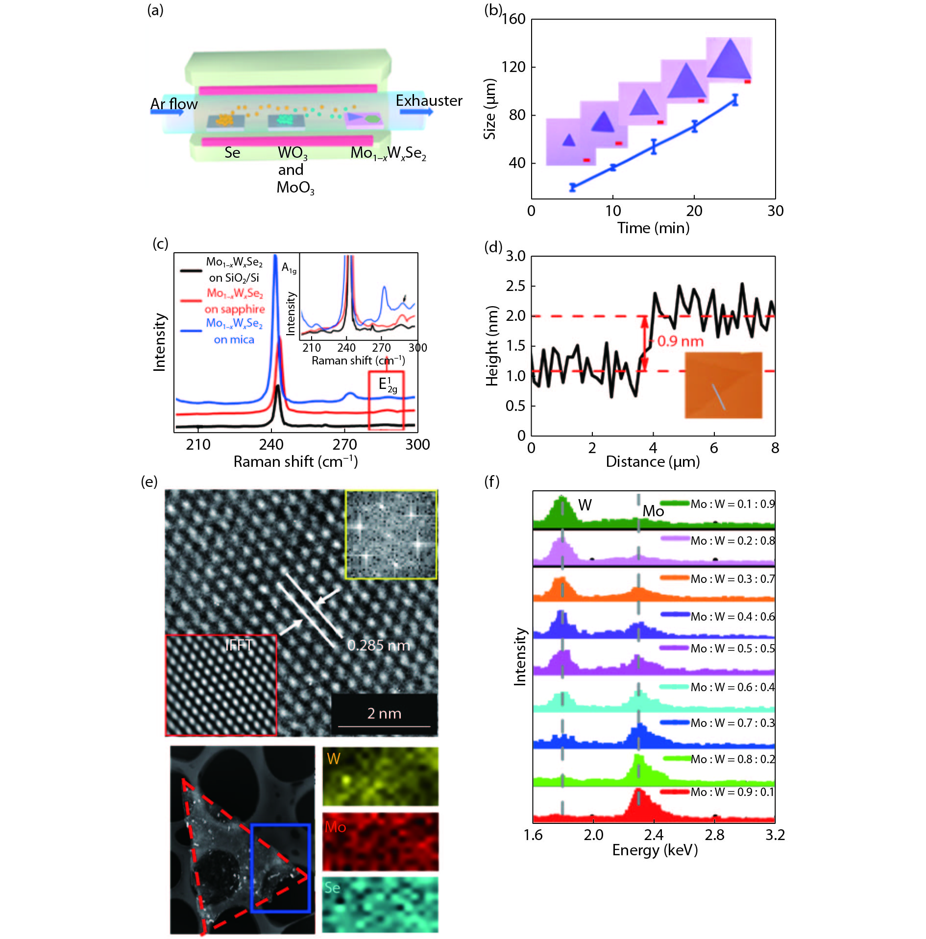
[28] X Zhang, S Xiao, L Shi et al. Large-size Mo1−
[29] T Y Ke, H P Hsu, Y P Wang et al. Temperature dependent piezoreflectance study of Mo1−
[30] M Yarali, H Brahmi, Z Yan et al. Effect of metal doping and vacancies on the thermal conductivity of monolayer molybdenum diselenide. ACS Appl Mater Inter, 10, 4921(2018).
[31] H Xu, X Wu, X Li et al. Properties of graphene-metal contacts probed by Raman spectroscopy. Carbon, 127, 491(2018).
[32] F Liang, H Xu, X Wu et al. Raman spectroscopy characterization of two-dimensional materials. Chin Phys B, 27, 037802(2018).
[33] C Luo, C Wang, X Wu et al. In situ transmission electron microscopy characterization and manipulation of two-dimensional layered materials beyond graphene. Small, 13, 1604259(2017).
[34] J Xia, X Huang, L Z Liu et al. CVD synthesis of large-area, highly crystalline MoSe2 atomic layers on diverse substrates and application to photodetectors. Nanoscale, 6, 8949(2014).
[35] J Huang, L Yang, D Liu et al. Large-area synthesis of monolayer WSe2 on a SiO2/Si substrate and its device applications. Nanoscale, 7, 4193(2015).


