
Fang Liang, Hejun Xu, Zuoyuan Dong, Yafeng Xie, Chen Luo, Yin Xia, Jian Zhang, Jun Wang, Xing Wu. Substrates and interlayer coupling effects on Mo1−xWxSe2 alloys[J]. Journal of Semiconductors, 2019, 40(6): 062005
- Journal of Semiconductors
- Vol. 40, Issue 6, 062005 (2019)
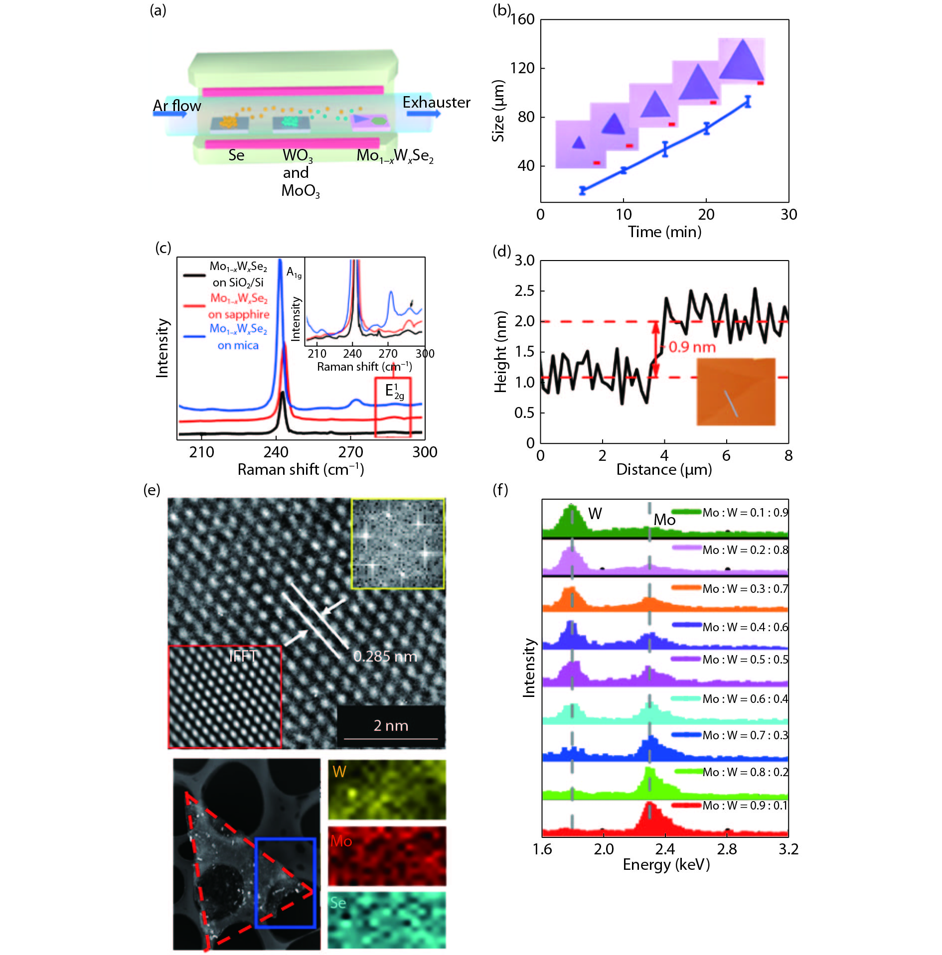
Fig. 1. (Color online) The synthesis and characterization of Mo1−x Wx Se2 alloys. (a) Schematic of the chemical vapor deposition setup for Mo1−x Wx Se2 alloys. (b) The time-dependent size curve of the Mo1−x Wx Se2 alloys grown by CVD on SiO2/Si. The insets show the triangle shape of the as-grown Mo1−x Wx Se2 alloys with different size. The scale bar is 5 μ m. (c) The Raman spectra of as-grown Mo1−x Wx Se2 alloys on different substrates. (d) AFM image of the as-grown Mo1−x Wx Se2 alloys. The AFM result shows that the thickness of the as-grown Mo1−x Wx Se2 is about 0.9 nm. (e) TEM result of as-grown Mo1−x Wx Se2 alloys. The bottom left shows the low-resolution TEM image and the bottom right shows the Mo, W, Se element mapping images of as-grown Mo1−x Wx Se2 alloys. The top view shows the HRTEM image of as-grown Mo1−x Wx Se2 alloys, the scale bar is 2 nm. The distance along the crystal plane (100) is 0.285 nm. The top right-hand inset of HRTEM image shows the corresponding selected area electron diffraction pattern (SAED), which demonstrates the as-grown Mo1−x Wx Se2 samples have the hexagon structure. The IFFT image in the bottom left-hand inset clearly demonstrates the result. (f) The EDX image of the as-grown Mo1−x Wx Se2 alloys. This image shows the Mo1−x Wx Se2 alloys with the different stoichiometric ratio of Mo and W.
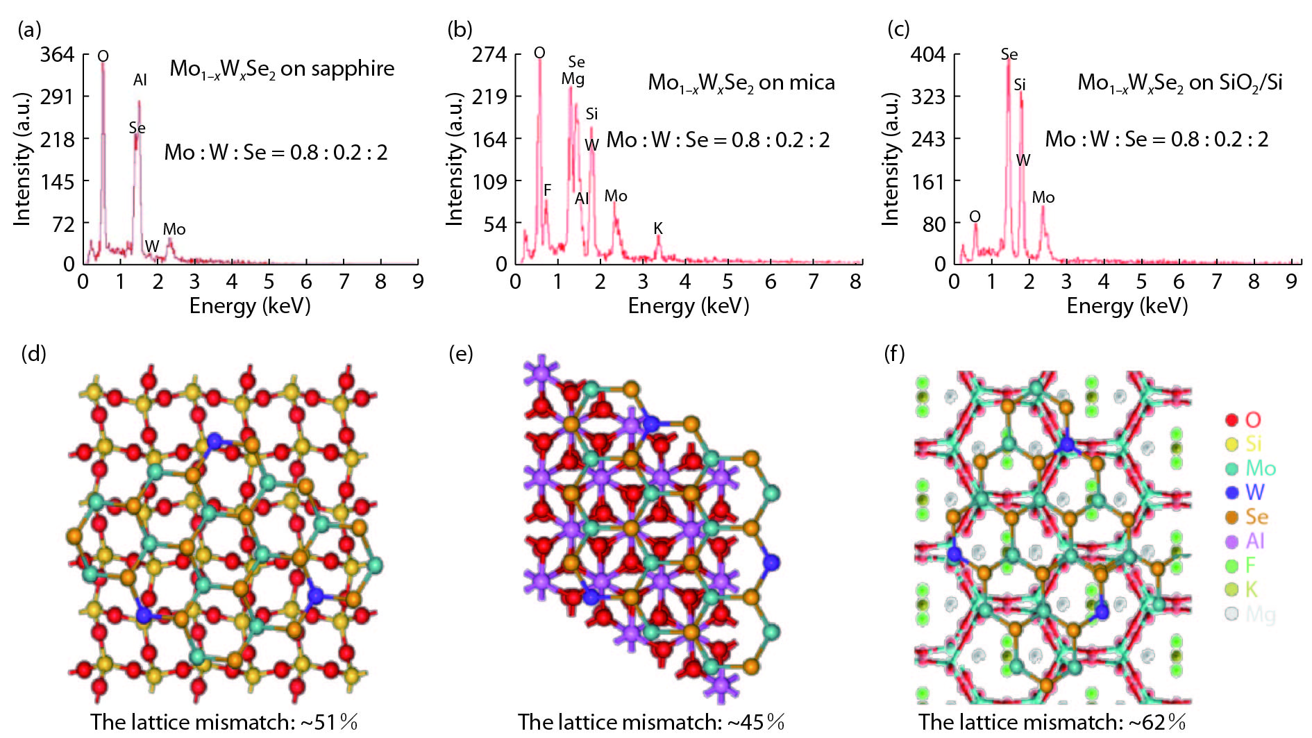
Fig. 2. (Color online) The EDX and lattice mismatch images of as-grown samples on different substrates. (a–c) show the EDX images of Mo0.8W0.2Se2 alloys grown on SiO2/Si, sapphire, and mica, respectively. (d–f) show the lattice mismatch images of Mo1−x Wx Se2 alloys on mica, SiO2/Si, sapphire, respectively. The lattice mismatches of Mo1−x Wx Se2 alloys with SiO2/Si, sapphire, and mica are about 51 %, 45 %, and 52 %, respectively.
Fig. 3. (Color online) The optical images of the as-grown Mo1−x Wx Se2 on different substrates and the corresponding AFM images. The optical images of Mo1−x Wx Se2 alloys grown on (a) SiO2/Si substrate, (b) mica substrate, (c) sapphire substrate. The scale bar is 5 μ m. (d–f) show the corresponding AFM images of the SiO2/Si, mica and sapphire, respectively. The RMS of the as-used SiO2/Si, mica and sapphire is 0.128, 0.058, and 0.137 nm, respectively. The scale bar is 0.5 μ m.
Fig. 4. (Color online) The PL characterization of the as-grown Mo1−x Wx Se2 alloys. (a) The PL image of the WSe2, Mo1−x Wx Se2 and MoSe2 grown on SiO2/Si substrates. (b) The PL image of monolayer Mo1−x Wx Se2 alloys grown on SiO2/Si, mica and sapphire. (c), (d) and (e) show the PL spectra of Mo1−x Wx Se2 alloys with different layers on sapphire, mica and SiO2/Si, respectively. The dashed lines in (c–e) help clearly to distinguish the variation tendency of the bandgaps over the thickness (f) Thickness-dependent PL spectra of Mo1−x Wx Se2 alloys on SiO2/Si, mica and sapphire substrates.


Set citation alerts for the article
Please enter your email address

© Copyright 2018-2021 | Chinese Laser Press. All Rights Reserved 沪ICP备15018463号-20