• Journal of Semiconductors
  • Vol. 40, Issue 6, 062005 (2019)
Fang Liang1, Hejun Xu1, Zuoyuan Dong1, Yafeng Xie2, Chen Luo1, Yin Xia1, Jian Zhang1, Jun Wang2, and Xing Wu1
Author Affiliations
  • 1Shanghai Key Laboratory of Multidimensional Information Processing, Department of Electronic Engineering, East China Normal University, Shanghai 200241, China
  • 2Laboratory of Micro-Nano Photonic and Optoelectronic Materials and Devices, Key Laboratory of Materials for High-Power Laser, Shanghai Institute of Optics and Fine Mechanics, Chinese Academy of Sciences, Shanghai 201800, China
  • show less
    DOI: 10.1088/1674-4926/40/6/062005 Cite this Article
    Fang Liang, Hejun Xu, Zuoyuan Dong, Yafeng Xie, Chen Luo, Yin Xia, Jian Zhang, Jun Wang, Xing Wu. Substrates and interlayer coupling effects on Mo1−xWxSe2 alloys[J]. Journal of Semiconductors, 2019, 40(6): 062005 Copy Citation Text show less

    Abstract

    Two-dimensional (2D) transition metal dichalcogenides alloys are potential materials in the application of photodetectors over a wide spectral range due to their composition-dependent bandgaps. The study of bandgap engineering is important for the application of 2D materials in devices. Here, we grow the Mo1-xWxSe2 alloys on mica, sapphire and SiO2/Si substrates by chemical vapor deposition (CVD) method. Mo1-xWxSe2 alloys are grown on the mica substrates by CVD method for the first time. Photoluminescence (PL) spectroscopy is used to investigate the effects of substrates and interlayer coupling force on the optical bandgaps of as-grown Mo1-xWxSe2 alloys. We find that the substrates used in this work have an ignorable effect on the optical bandgaps of as-grown Mo1-xWxSe2. The interlayer coupling effect on the optical bandgaps of as-grown Mo1-xWxSe2 is larger than the substrates effect. These findings provide a new way for the future study of the growth and physical properties of 2D alloy materials.

    1. Introduction

    Two-dimensional (2D) materials, such as black phosphorus (BP)[1], topological insulators[2], transition metal dichalcogenides (TMDs) materials[38], have become popular research topics since graphene was discovered by Novoselov et al. in 2004[9]. TMD-layered materials with graphene-like structures have potential applications in digital electronics, optoelectronics devices and thermoelectrical fields due to their outstanding electronic, optical, and thermal properties. TMD-layered materials, such as MoSe2 and WSe2, have strong light-matter interactions and broad-band light absorption, and are promising materials for use in constructing various photodetectors[10, 11]. However, several works have reported that binary TMD-layered materials may introduce defects, such as chalcogen vacancies. Unfortunately, these defects usually serve as localized deep-level defect states[1214], which have an enormous influence on the photoresponse of photodetectors. Yao et al.[13] have reported that localized deep-level defect states can be effectively suppressed by alloys.

    Both theoretical and experimental studies[1521] indicate that layered-TMD alloys have bandgaps that can be tuned by adjusting the composition of the corresponding atoms. Moreover, the thermodynamic properties of layered-TMD alloys are theoretically more stable than their binary counterparts. Thus, layered-TMD alloys, which have composition-dependent bandgaps, are able to extend the use of 2D materials in photodetectors over a wide spectral range. However, currently, only several TMD ternary alloys, such as MoSe2(1−x)S2x[20, 22],WS2xSe2−2x[23], Mo1−xWxSe2[2428], and Mo1−xWxSe2[17, 29, 30], have been studied experimentally. There is still no systematic study on the Mo1−xWxSe2 alloys due to the difficulty of their synthesis.

    In this work, the Mo1−xWxSe2 alloys are synthesized on mica, sapphire and SiO2/Si substrates by the chemical vapor deposition (CVD) method. The Mo1−xWxSe2 alloys are first synthesized on the mica substrates by the CVD method. The effects of substrates and interlayer coupling force on the as-grown Mo1−xWxSe2 alloys are then investigated by an atomic force microscope (AFM), Raman spectroscopy and photoluminescence (PL) spectroscopy. The results show that the as-used substrates have negligible effects on the bandgaps of the Mo1−xWxSe2 alloys, while the interlayer coupling effect on the optical bandgaps of Mo1−xWxSe2 alloys is greater than the substrates.

    2. Result and discussion

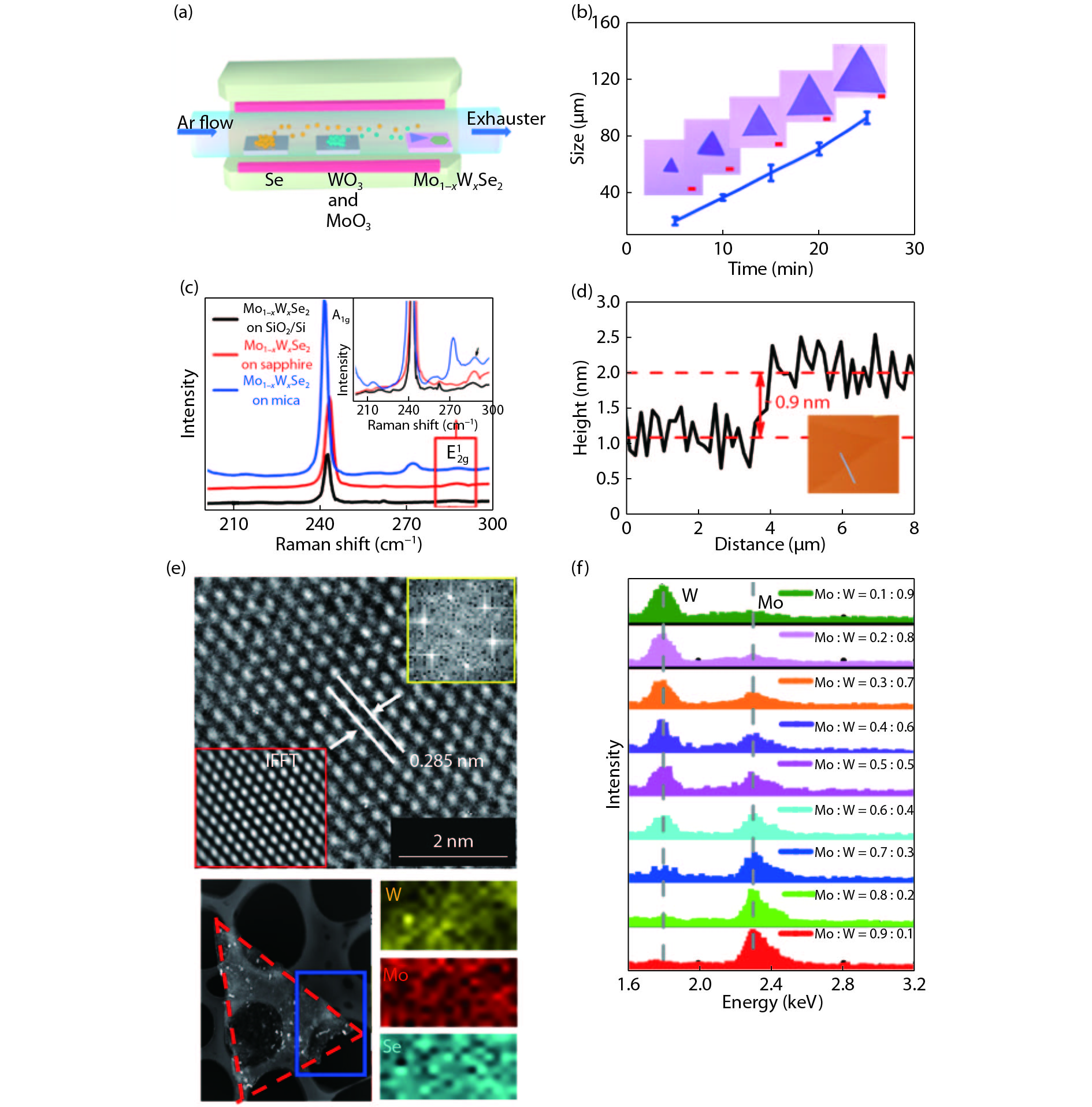
    The Mo1−xWxSe2 alloys are prepared on different substrates and are synthesized using the CVD method. The details are introduced in the method section. A schematic of the CVD growing setup is shown in Fig. 1(a). The size of Mo1−xWxSe2 alloys on SiO2/Si substrates as a function of the growing time is illustrated in Fig. 1(b), which reveals that the size of Mo1–xWxSe2 alloys increases with the incremental growth time within 25 min. Raman spectroscopy is a fast and accurate but nondestructive tool to study material structures and properties[31, 32]. The Raman spectra of Mo1−xWxSe2 alloys on different substrates are shown in Fig. 1(c). The prominent peaks occurring around 241 cm-1 are the A1g Raman modes of as-grown Mo1−xWxSe2 alloys. The inset in Fig. 1(c) shows the weak E2g1 peaks of Mo1−xWxSe2 alloys on different substrates. The A1g and E2g1 modes of Mo1−xWxSe2 samples grown on the three different substrates have negligible differences in their peak positions. AFM is the most effective means to identify the number of layers of materials and study the surface structures of samples. The AFM image in Fig. 1(d) shows the thickness of the as-grown Mo1−xWxSe2 alloy is about 0.9 nm, which indicates that the as-grown Mo1−xWxSe2 alloy is a monolayer. The inset image with homogeneous color contrast in Fig. 1(d) indicatesthat the as-grown sample has a flat and uniform surface. TEM characterization technique is a powerful tool to study the crystal structures and composition information of 2D materials[33]. The low-resolution TEM image in the bottom left-hand panel of Fig. 1(e) clearly shows that the Mo1−xWxSe2 sample on the copper grid meshes with the triangular shape. The sample inside the blue rectangle is chosen for element mapping and HRTEM (high-resolution transmission electron microscopy). The Mo, W, Se element mapping images in the bottom left-hand panel of Fig. 1(e) show the as-grown Mo1−xWxSe2 alloys contain the Mo, W and Se atoms and indicate the uniform distribution of Mo, W, and Se atoms in the samples. The HRTEM image in the top view of Fig. 1(e) shows the clear atomic structure of as-grown Mo1−xWxSe2 alloys. The lattice constant of the Mo1−xWxSe2 alloy is 0.285 nm, which is between the lattice constant of MoSe2 (0.28 nm)[34] and WSe2 (0.33 nm)[35]. The top right inset of HRTEM image shows the corresponding selected area electron diffraction pattern (SAED), which demonstrates that the as-grown Mo1−xWxSe2 samples have hexagon structure with good crystallinity. This result is further confirmed with the IFFT image in the bottom left-hand panel inset. There is only one set of diffraction pattern in the SAED image. The SAED image and Mo, W, Se element mapping images demonstrate the as-grown samples are Mo1−xWxSe2 alloys rather than the heterostructures and binary counterparts. The energy dispersive X-ray spectroscopy (EDX) can be used to measure the relative content of the elements of materials. Fig. 1(f) shows the EDX image of Mo1−xWxSe2 alloys with different stoichiometric ratio of Mo and W. The stoichiometric ratio of Mo and W changes from 0.1 : 0.9 to 0.9 : 0.1. The stoichiometric ratio of Mo and W changes from the mixture ratio of WO3 and MoO3 powders used as the precursors in the CVD method.

    (Color online) The synthesis and characterization of Mo1−xWxSe2 alloys. (a) Schematic of the chemical vapor deposition setup for Mo1−xWxSe2 alloys. (b) The time-dependent size curve of the Mo1−xWxSe2 alloys grown by CVD on SiO2/Si. The insets show the triangle shape of the as-grown Mo1−xWxSe2 alloys with different size. The scale bar is 5 μm. (c) The Raman spectra of as-grown Mo1−xWxSe2 alloys on different substrates. (d) AFM image of the as-grown Mo1−xWxSe2 alloys. The AFM result shows that the thickness of the as-grown Mo1−xWxSe2 is about 0.9 nm. (e) TEM result of as-grown Mo1−xWxSe2 alloys. The bottom left shows the low-resolution TEM image and the bottom right shows the Mo, W, Se element mapping images of as-grown Mo1−xWxSe2 alloys. The top view shows the HRTEM image of as-grown Mo1−xWxSe2 alloys, the scale bar is 2 nm. The distance along the crystal plane (100) is 0.285 nm. The top right-hand inset of HRTEM image shows the corresponding selected area electron diffraction pattern (SAED), which demonstrates the as-grown Mo1−xWxSe2 samples have the hexagon structure. The IFFT image in the bottom left-hand inset clearly demonstrates the result. (f) The EDX image of the as-grown Mo1−xWxSe2 alloys. This image shows the Mo1−xWxSe2 alloys with the different stoichiometric ratio of Mo and W.

    Figure 1.(Color online) The synthesis and characterization of Mo1−xWxSe2 alloys. (a) Schematic of the chemical vapor deposition setup for Mo1−xWxSe2 alloys. (b) The time-dependent size curve of the Mo1−xWxSe2 alloys grown by CVD on SiO2/Si. The insets show the triangle shape of the as-grown Mo1−xWxSe2 alloys with different size. The scale bar is 5 μm. (c) The Raman spectra of as-grown Mo1−xWxSe2 alloys on different substrates. (d) AFM image of the as-grown Mo1−xWxSe2 alloys. The AFM result shows that the thickness of the as-grown Mo1−xWxSe2 is about 0.9 nm. (e) TEM result of as-grown Mo1−xWxSe2 alloys. The bottom left shows the low-resolution TEM image and the bottom right shows the Mo, W, Se element mapping images of as-grown Mo1−xWxSe2 alloys. The top view shows the HRTEM image of as-grown Mo1−xWxSe2 alloys, the scale bar is 2 nm. The distance along the crystal plane (100) is 0.285 nm. The top right-hand inset of HRTEM image shows the corresponding selected area electron diffraction pattern (SAED), which demonstrates the as-grown Mo1−xWxSe2 samples have the hexagon structure. The IFFT image in the bottom left-hand inset clearly demonstrates the result. (f) The EDX image of the as-grown Mo1−xWxSe2 alloys. This image shows the Mo1−xWxSe2 alloys with the different stoichiometric ratio of Mo and W.

    Figs. 2(a)2(c) show the EDX image of Mo0.8W0.2Se2 alloys on SiO2/Si, sapphire and mica, respectively. These images show that the substrates have no effect on the stoichiometric ratio of the Mo0.8W0.2Se2 alloys. Figs. 2(d)2(f) show the lattice mismatch images of Mo1−xWxSe2 alloys on mica, SiO2/Si, and sapphire, respectively. The lattice mismatches of Mo1−xWxSe2 alloys with SiO2/Si, sapphire, and mica are about 51 %, 45 % and 52 %, respectively. Figs. 3(a)3(c) show the optical images observed by the optical microscopy of Mo1−xWxSe2 alloys grown on SiO2/Si, mica, sapphire substrates, respectively. Optical microscopy is the simplest and most effective method to characterize the layered materials. The layer number of the materials can be first identified by the optical microscope. Figs. 3(d)3(f) show the AFM images of the SiO2/Si, mica, and sapphire, respectively. The root-mean-square (RMS) of the roughness of as-used SiO2/Si, mica and sapphire is 0.128, 0.058, and 0.137 nm, respectively. Thus, mica can provide the smoothest surface among the three substrates for material synthesis.

    (Color online) The EDX and lattice mismatch images of as-grown samples on different substrates. (a–c) show the EDX images of Mo0.8W0.2Se2 alloys grown on SiO2/Si, sapphire, and mica, respectively. (d–f) show the lattice mismatch images of Mo1−xWxSe2 alloys on mica, SiO2/Si, sapphire, respectively. The lattice mismatches of Mo1−xWxSe2 alloys with SiO2/Si, sapphire, and mica are about 51 %, 45 %, and 52 %, respectively.

    Figure 2.(Color online) The EDX and lattice mismatch images of as-grown samples on different substrates. (a–c) show the EDX images of Mo0.8W0.2Se2 alloys grown on SiO2/Si, sapphire, and mica, respectively. (d–f) show the lattice mismatch images of Mo1−xWxSe2 alloys on mica, SiO2/Si, sapphire, respectively. The lattice mismatches of Mo1−xWxSe2 alloys with SiO2/Si, sapphire, and mica are about 51 %, 45 %, and 52 %, respectively.

    (Color online) The optical images of the as-grown Mo1−xWxSe2 on different substrates and the corresponding AFM images. The optical images of Mo1−xWxSe2 alloys grown on (a) SiO2/Si substrate, (b) mica substrate, (c) sapphire substrate. The scale bar is 5 μm. (d–f) show the corresponding AFM images of the SiO2/Si, mica and sapphire, respectively. The RMS of the as-used SiO2/Si, mica and sapphire is 0.128, 0.058, and 0.137 nm, respectively. The scale bar is 0.5 μm.

    Figure 3.(Color online) The optical images of the as-grown Mo1−xWxSe2 on different substrates and the corresponding AFM images. The optical images of Mo1−xWxSe2 alloys grown on (a) SiO2/Si substrate, (b) mica substrate, (c) sapphire substrate. The scale bar is 5 μm. (d–f) show the corresponding AFM images of the SiO2/Si, mica and sapphire, respectively. The RMS of the as-used SiO2/Si, mica and sapphire is 0.128, 0.058, and 0.137 nm, respectively. The scale bar is 0.5 μm.

    PL spectroscopy is a direct method to characterize the optical bandgaps of 2D materials. Fig. 4(a) shows the PL spectra of WSe2, Mo1−xWxSe2 and MoSe2on SiO2/Si substrates. The PL spectrum of Mo1−xWxSe2 located at 1543 meV is in the range between that of WSe2 located at 1592 meV and MoSe2 located at 1510 meV. This result further demonstrates the as-grown samples are alloys. Fig. 4(b) show the PL spectra of monolayer Mo1−xWxSe2 alloys grown on SiO2/Si, mica and sapphire substrates. The changes of PL spectra of Mo1−xWxSe2 alloys on these three substrates are merely about several meV, which demonstrates that the substrates have negligible effects on the optical bandgaps of as-grown Mo1−xWxSe2 alloys. This finding provides an instructive idea for the choice of substrates to grow the alloys by CVD method. Figs. 4(c)4(e) show the PL spectra of Mo1−xWxSe2 alloys with different layers on sapphire, mica and SiO2/Si, respectively. The bandgaps redshift as the layer numbers of the samples increase, which demonstrates that the interlayer coupling effects related to the layer numbers have large effects on the optical bandgaps of Mo1−xWxSe2 alloys. Fig. 4(f) show the corresponding thickness-dependent PL spectra of Mo1−xWxSe2 alloys on SiO2/Si, mica and sapphire from Figs. 4(c)4(e). The peak position variations of Mo1−xWxSe2 alloys with different thickness are larger than the Mo1−xWxSe2 alloys growing on different three substrates. Our results demonstrate that the interlayer coupling effect on the optical bandgaps of Mo1−xWxSe2 alloys is greater than the substrates effect.

    (Color online) The PL characterization of the as-grown Mo1−xWxSe2 alloys. (a) The PL image of the WSe2, Mo1−xWxSe2 and MoSe2 grown on SiO2/Si substrates. (b) The PL image of monolayer Mo1−xWxSe2 alloys grown on SiO2/Si, mica and sapphire. (c), (d) and (e) show the PL spectra of Mo1−xWxSe2 alloys with different layers on sapphire, mica and SiO2/Si, respectively. The dashed lines in (c–e) help clearly to distinguish the variation tendency of the bandgaps over the thickness (f) Thickness-dependent PL spectra of Mo1−xWxSe2 alloys on SiO2/Si, mica and sapphire substrates.

    Figure 4.(Color online) The PL characterization of the as-grown Mo1−xWxSe2 alloys. (a) The PL image of the WSe2, Mo1−xWxSe2 and MoSe2 grown on SiO2/Si substrates. (b) The PL image of monolayer Mo1−xWxSe2 alloys grown on SiO2/Si, mica and sapphire. (c), (d) and (e) show the PL spectra of Mo1−xWxSe2 alloys with different layers on sapphire, mica and SiO2/Si, respectively. The dashed lines in (c–e) help clearly to distinguish the variation tendency of the bandgaps over the thickness (f) Thickness-dependent PL spectra of Mo1−xWxSe2 alloys on SiO2/Si, mica and sapphire substrates.

    3. Conclusion

    In conclusion, Mo1−xWxSe2 films are synthesized on sapphire, mica and SiO2/Si substrates by the CVD method. The AFM, Raman and PL characterization techniques are used to ascertain the monolayer nature of the as-grown samples. The EDX spectra show the adjustable stoichiometric ratio of the 2D alloy materials synthesized by the CVD method. The TEM results indicate the high quality and homogeneity of the as-grown samples. The Raman and AFM results show the roughness of the substrates have a negligible effect on the E2g1 of the Mo1−xWxSe2 alloys. The PL results indicate that the substrates have negligible effects on the bandgaps of Mo1−xWxSe2 alloys and also show that the interlayer coupling effect related to the layer numbers on the optical bandgaps of Mo1−xWxSe2 alloys is larger than the substrates effect. These findings prove a new way for the future study of the growth dynamics and physical properties of two-dimensional materials.

    Acknowledgements

    This work was supported by the National Natural Science Foundation of China (Nos. 11504111, 61574060), the Projects of Science and Technology Commission of Shanghai Municipality (Nos. 15JC1401800, 14DZ2260800), the Program for Professor of Special Appointment (Eastern Scholar), the Shanghai Rising-Star Program (No. 17QA1401400), the Young Elite Scientists Sponsorship (YESS) Program by CAST, and the Fundamental Research Funds for the Central Universities.

    Appendix A

    Synthesis of Mo1xWxSe2films:Mo1−xWxSe2 films are synthesized in a CVD furnace (Thermo Scientific Lindberg/Blue M Moldatherm) with a one-inch diameter quartz tube. Se powders (99.99 %, Sigma-Aldrich) put in a quartz boat are placed upstream at the edge of the furnace. The mixture MoO3 powders (99.9 %, Sigma-Aldrich) and WO3 powders (99.9 %, Sigma-Aldrich) are put in the center of the face-to-face substrates. The substrates (mica, sapphire, 300 nm SiO2/Si) with a mixture of MoO3 and WO3powders are put on a quartz sheet and are then placed in the heating center. The velocity of carrier gas argon (Ar) is kept for 80 to 100 standard cubic centimeters per minute (sccm) after purifying the system with 200 sccm Ar for 30 min. The furnace is heated to 900 °C with a heating rate of 20 °C/min and keeps at 900 °C for 15 min. After the growth process is completed, the furnace is cooled to room temperature.

    Characterization: Optical images are obtained by using an optical microscope (OLYMPUS BX41M-LED). Raman spectra and PL spectra are tested by using a Raman spectroscopy (Horiba, LabRAM HR-800) with a laser excitation wavelength of 532 nm. The grating for Raman spectra is 1800 I/mm and for PL spectra is 300 I/mm. The laser beam is focused on the samples to a diameter of ~ 2 μm by a × 50 objective. The laser power is adjusted at a power of ~ 3.7 mW to minimize the laser-induced thermal effect. EDX characterization is carried out on an FEI XL30 ESEM facility with the acceleration voltage of 10 kV. The surface morphology and layer numbers are characterized by AFM technique (MicroNano D-5A). TEM samples are prepared by using a PMMA assisted transfer technology. The TEM images are recorded at 200 kV on a JEOL 2100F.

    References

    [1] G Zhang, S Huang, A Chaves et al. Infrared fingerprints of few-layer black phosphorus. Nat Commun, 8, 14071(2017).

    [2] M Mogi, M Kawamura, R Yoshimi et al. A magnetic heterostructure of topological insulators as a candidate for an axion insulator. Nat Mater, 16, 516(2017).

    [3] Y Zhang, T R Chang, B Zhou et al. Direct observation of the transition from indirect to direct bandgap in atomically thin epitaxial MoSe2. Nat Nanotechnol, 9, 111(2014).

    [4] S Bertolazzi, M Gobbi, Y Zhao et al. Molecular chemistry approaches for tuning the properties of two-dimensional transition metal dichalcogenides. Chem Soc Rev, 47, 6845(2018).

    [5] P Manimunda, Y Nakanishi, Y M Jaques et al. Nanoscale deformation and friction characteristics of atomically thin WSe2 and heterostructure using nanoscratch and Raman spectroscopy. 2D Mater, 4, 045005(2017).

    [6] C Wang, X Wu, Y Ma et al. Metallic few-layered VSe2 nanosheets: high two-dimensional conductivity for flexible in-plane solid-state supercapacitors. J Mater Chem A, 6, 8299(2018).

    [7] S Xiao, P Xiao, X Zhang et al. Atomic-layer soft plasma etching of MoS2. Sci Rep, 6, 19945(2016).

    [8] X Zhang, H Nan, S Xiao et al. Shape-uniform, high-quality monolayered MoS2 crystals for gate-tunable photoluminescence. ACS Appl Mater Inter, 9, 42121(2017).

    [9] K S Novoselov, A K Geim, S V Morozov et al. Electric field effect in atomically thin carbon flims. Science, 306, 666(2004).

    [10] Z Zheng, J Yao, G Yang. Centimeter-scale deposition of Mo0.5W0.5Se2 alloy film for high-performance photodetectors on versatile substrates. ACS Appl Mater Inter, 9, 14920(2017).

    [11] J Liu, M Zhong, X Liu et al. Two-dimensional plumbum-doped tin diselenide monolayer transistor with high on/off ratio. Nanotech, 29, 474002(2018).

    [12] W Zhou, X Zou, S Najmaei et al. Intrinsic structural defects in monolayer molybdenum disulfide. Nano Lett, 13, 2615(2013).

    [13] J Yao, Z Zheng, G Yang. Promoting the performance of layered-material photodetectors by alloy engineering. ACS Appl Mater Inte, 8, 12915(2016).

    [14] C P Lu, G Li, J Mao et al. Bandgap, mid-gap states, and gating effects in MoS2. Nano Lett, 14, 4628(2014).

    [15] J Kang, S Tongay, J Li et al. Monolayer semiconducting transition metal dichalcogenide alloys: Stability and band bowing. J Appl Phys, 113, 143703(2013).

    [16] Q Peng, S De. Tunable band gaps of mono-layer hexagonal BNC heterostructures. Physica E, 44, 1662(2012).

    [17] J Ye, B Niu, Y Li et al. Exciton valley dynamics in monolayer Mo1−xWxSe2 (x = 0, 0.5, 1). Appl Phys Lett, 111, 152106(2017).

    [18] C Zhang, S Kc, Y Nie et al. Charge mediated reversible metal−insulator transition in monolayer MoTe2 and WxMo1−xTe2 alloy. ACS Nano, 10, 7370(2016).

    [19] T Livneh, D O Dumcenco, I Pinkas. Determining alloy composition in MoxW(1−x)S2 from low wavenumber Raman spectroscopy. J Raman Spectrosc, 48, 773(2017).

    [20] H Li, Q Zhang, X Duan et al. Lateral growth of composition graded atomic layer MoS(2(1−x))Se(2x) nanosheets. J Am Chem Soc, 137, 5284(2015).

    [21] J Liu, X Liu, Z Chen et al. Tunable Schottky barrier width and enormously enhanced photoresponsivity in Sb doped SnS2 monolayer. Nano Res, 12, 463(2018).

    [22] H Li, X Duan, X Wu et al. Growth of alloy MoS(2x)Se2(1−x) nanosheets with fully tunable chemical compositions and optical properties. J Am Chem Soc, 136, 3756(2014).

    [23] X Duan, C Wang, Z Fan et al. Synthesis of WS2xSe2−2x alloy nanosheets with composition-tunable electronic properties. Nano Lett, 16, 264(2016).

    [24] Y Chen, D O Dumcenco, Y Zhu et al. Composition-dependent Raman modes of Mo(1−x)W(x)S2 monolayer alloys. Nanoscale, 6, 2833(2014).

    [25] D O Dumcenco, H Kobayashi, Z Liu et al. Visualization and quantification of transition metal atomic mixing in Mo1−xWxSe2 single layers. Nat Commun, 4, 1351(2013).

    [26] J G Song, G H Ryu, S J Lee et al. Controllable synthesis of molybdenum tungsten disulfide alloy for vertically composition-controlled multilayer. Nat Commun, 6, 7817(2015).

    [27] D O Dumcenco, K Y Chen, Y P Wang et al. Raman study of 2H-Mo1−xWxS2 layered mixed crystals. J Alloy Compd, 506, 940(2010).

    [28] X Zhang, S Xiao, L Shi et al. Large-size Mo1−xWxS2 and Mo1−xWxS2 (x = 0−0.5) monolayers by confined-space chemical vapor deposition. Appl Surf Sci, 457, 591(2018).

    [29] T Y Ke, H P Hsu, Y P Wang et al. Temperature dependent piezoreflectance study of Mo1−xWxSe2 layered crystals. J Appl Phys, 118, 215704(2015).

    [30] M Yarali, H Brahmi, Z Yan et al. Effect of metal doping and vacancies on the thermal conductivity of monolayer molybdenum diselenide. ACS Appl Mater Inter, 10, 4921(2018).

    [31] H Xu, X Wu, X Li et al. Properties of graphene-metal contacts probed by Raman spectroscopy. Carbon, 127, 491(2018).

    [32] F Liang, H Xu, X Wu et al. Raman spectroscopy characterization of two-dimensional materials. Chin Phys B, 27, 037802(2018).

    [33] C Luo, C Wang, X Wu et al. In situ transmission electron microscopy characterization and manipulation of two-dimensional layered materials beyond graphene. Small, 13, 1604259(2017).

    [34] J Xia, X Huang, L Z Liu et al. CVD synthesis of large-area, highly crystalline MoSe2 atomic layers on diverse substrates and application to photodetectors. Nanoscale, 6, 8949(2014).

    [35] J Huang, L Yang, D Liu et al. Large-area synthesis of monolayer WSe2 on a SiO2/Si substrate and its device applications. Nanoscale, 7, 4193(2015).

    Fang Liang, Hejun Xu, Zuoyuan Dong, Yafeng Xie, Chen Luo, Yin Xia, Jian Zhang, Jun Wang, Xing Wu. Substrates and interlayer coupling effects on Mo1−xWxSe2 alloys[J]. Journal of Semiconductors, 2019, 40(6): 062005
    Download Citation