
Xiao Yang, Yue Lin, Tingzhu Wu, Zijun Yan, Zhong Chen, Hao-Chung Kuo, Rong Zhang. An overview on the principle of inkjet printing technique and its application in micro-display for augmented/virtual realities[J]. Opto-Electronic Advances, 2022, 5(6): 210123
- Opto-Electronic Advances
- Vol. 5, Issue 6, 210123 (2022)
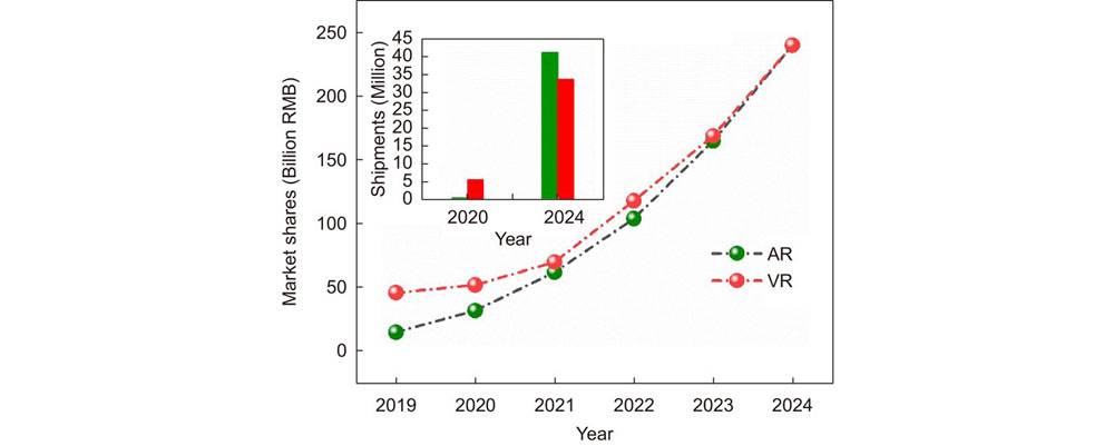
Fig. 1. The growth of market share of AR/VR1.
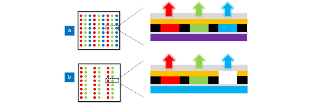
Fig. 2. Two methods for achieving full-color by using QD CCL . (a ) RBG three-color QDs excited by UV chips. (b ) RG two-color QDs excited by blue chips.
Fig. 3. Structures of realizing the NRET from chip to QDs33. Figure reproduced with permission from John Wiley and Sons.
Fig. 4. (a ) Schematic diagram of AJP process. (b ) Processes of fabricating the full-color micro-LED display based on lithography and AJP technique. (c ) Full-color design of QD-NR-Micro-LED display. Figure reproduced with permission from: (a) ref.16, The Optical Society; (b) ref.41, (c) ref.15, Chinese Laser Press.
Fig. 5. (a ) Sketch of the full color RGB QD-converted micro-LED array based on an UV backlight module and the device image (inset). (b ) Schematic illustration of the full-color prototype . (c ) Cross-section structure diagram of the prototype. Figure reproduced with permission from: (a) ref.42, American Chemical Society; (b, c) ref.45, John Wiley and Sons.
Fig. 6. Fluorescence images of (a ) NCTU and (b ) logo of XMU printed by SIJ printing. Figure reproduced with permission from: (a)15, Optica Publishing Group.
Fig. 7. A distribution of line widths of various inkjet printing in recent decades16–19, 42–44, 48, 50, 52–115.
Fig. 8. (a ) Photographs of the CsPbX3 inks. (b ) CsPbX3 films with different halide compositions under a 365 nm UV lamp and (c ) schematic of perovskite transformation from CsPbX3 ink to CsPbX3 nanocrystal. Figure reproduced with permission from ref.19, John Wiley and Sons.
Fig. 9. (a ) Schematic diagram of the in situ inkjet printing strategy. (b ) The optical images of printed PQD patterns on different polymer substrates under UV light. Figure reproduced with permission from ref.69, John Wiley and Sons.
Fig. 10. (a ) Relationships between the concentrations of silica particles in colloidal inks and the contact angles of ITO glasses and silicon wafers with Teflon layers. Optical images of the latex droplets and printed photonic crystals microstructures on the ITO glasses and silicon wafers with Teflon layers. (b ) Schematic illustration of the film forming process using thermal-curing and UV-curing inks, respectively. (c ) PL microscopic images and 3D morphology images of dot arrays, and film thickness profile of each single dot achieved by printing quantum dots inks with volume ratios of 0, 10, 20, and 30% oDBC. (d ) Fluid flow schematic of the AJP system with a dual atomizer module91. (e ) Fabricated 2D patterning of a square grid on planar surfaces91. (f ) LZH logo printed on a freeform cylindrical surface121. Figure reproduced with permission from: (a) ref.113, American Chemical Society; (b) ref.43, John Wiley and Sons; (c) ref.17, American Chemical Society; (d–f) ref.91, AIP Publishing.
Fig. 11. (a ) Schematic illustration of the EHD inkjet printing fabrication process and perovskite transformation. (b ) The EHD printed high-resolution dot array with dot diameters of 1, 2, and 3 µm respectively. (c ) Printing mode of conventional EHD inkjet printing (1) vs SIJ (2) shown with and without ink charging. (d ) Three-dimensional AFM image of aligned arrays of dots. (e ) Continuous lines printed using the single-walled carbon nanotube ink. (f ) Optical micrograph of a portrait of an ancient scholar, Hypatia, printed using a polyurethane ink. (g ) Schematic of the concave (trench) formation. (h ) Topographical AFM images demonstrating the mass transfer of a PAz film under UV-light irradiation and changes in the cross-sectional profile obtained from the AFM data. Figure reproduced with permission from: (a, b) ref.107, John Wiley and Sons; (c) ref.24; (d–f) 75, Springer Nature; (g, h) ref.88, under a Creative Commons Attribution 4.0 International License.
Fig. 12. (a ) Fluorescence microphotographs and three-dimensional white light interferometer images of dot arrays printed with different PVP concentrations. (b ) Fluorescence microphotographs, higher resolution fluorescence microphotographs and 3D morphology images of the white light interferometer of QD dot arrays. (c ) Illustration depicting deposition mechanism and binarized experimental images of deposits of spheres, slightly stretched particles and ellipsoids. (d ) SEM images of polystyrene ink drops printed in one, two, and three layers; AFM profile of deposited drops of PS 450. (e ) Cross section and 3D projection from an optical profilometer of single drops at different temperatures. (f ) Confocal laser scattering microscopic 3D images of dots with varying solvent compositions and corresponding two-dimensional profiles. Figure reproduced with permission from: (a) ref.112, The Royal Society of Chemistry; (b) ref.71, John Wiley and Sons; (c) ref.126, American Physical Society; (d) ref.127, John Wiley and Sons; (e) ref.128, American Chemical Society; (f) ref.129, AIP Publishing.
Fig. 13. (a ) Schematic illustration and optical microscopy images of the perovskite precursor droplet crystallizing on high and low adhesion substrates62. (b ) The fluorescence and the contact angle images of resulting microdisks printed at different temperatures from 30 to 90 °C69. (c ) Controllability of 3D microstructures by IJP on surfaces with tunable dewettability130. (d ) Suppression of the coffee stain effect illustrated with different materials at three frequencies and amplitude modulation131.
|
Table 0. The differences between different printing methods.
|

Set citation alerts for the article
Please enter your email address
© Copyright 2018-2021 | Chinese Laser Press. All Rights Reserved 沪ICP备15018463号-20