1Department of Electronic Science, Fujian Engineering Research Center for Solid-State Lighting, Xiamen University, Xiamen 361005, China
2Institute of Future Display Technology, Xiamen University, Xiamen 361005, China
3Department of Photonics & Graduate Institute of Electro-Optical Engineering, College of Electrical and Computer Engineering, Chiao Tung University, Hsinchu 30010, Taiwan, China
Xiao Yang, Yue Lin, Tingzhu Wu, Zijun Yan, Zhong Chen, Hao-Chung Kuo, Rong Zhang. An overview on the principle of inkjet printing technique and its application in micro-display for augmented/virtual realities[J]. Opto-Electronic Advances, 2022, 5(6): 210123
Copy Citation Text
Augmented reality (AR) and virtual reality (VR) are two novel display technologies that are under updates. The essential feature of AR/VR is the full-color display that requires high pixel densities. To generate three-color pixels, the fluorescent color conversion layer inevitably includes green and red pixels. To fabricate such sort of display kits, inkjet printing is a promising way to position the color conversion layers. In this review article, the progress of AR/VR technologies is first reviewed, and in succession, the state of the art of inkjet printing, as well as two key issues — the optimization of ink and the reduction of coffee-ring effects, are introduced. Finally, some potential problems associated with the color converting layer are highlighted.Augmented reality (AR) and virtual reality (VR) are two novel display technologies that are under updates. The essential feature of AR/VR is the full-color display that requires high pixel densities. To generate three-color pixels, the fluorescent color conversion layer inevitably includes green and red pixels. To fabricate such sort of display kits, inkjet printing is a promising way to position the color conversion layers. In this review article, the progress of AR/VR technologies is first reviewed, and in succession, the state of the art of inkjet printing, as well as two key issues — the optimization of ink and the reduction of coffee-ring effects, are introduced. Finally, some potential problems associated with the color converting layer are highlighted.
Introduction
Progress of augmented/virtual realities
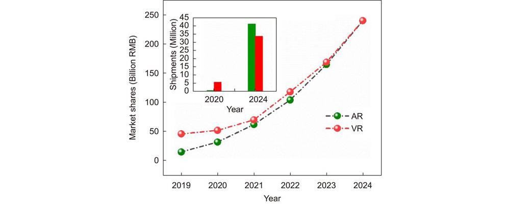
With the rapid development of artificial intelligence, image recognition and 5G communication technology, augmented reality (AR) and virtual reality (VR) technologies are growing at remarkable rates. Tech giants, such as Facebook, Google, Samsung Electronics and Apple, have been investing in the AR/VR industry. Specifically, near-eye displays (NEDs) and head-mounted displays (HMDs) are seed equipment studied by major technology companies and research institutes. In 2020, the outbreak of COVID-19 led to the stagnation of the global market economy. On the other hand, the pandemic provided an opportunity for the development of AR/VR technology. COVID-19 started a new era of remote office interaction and remote consumer interaction, and the market once again turned its attention to VR and increased investment in technology applications. For future development, AR/VR technology will be the key to improving human living standards and quality. The breakthrough of this technology will also elevate human civilization to a new level. According to International Data Corporation (IDC), a market research institution, the market scale of the global AR and VR industries will both grow from approximately ¥28 billion and ¥62 billion, respectively, in 2020, to ¥240 billion in 2024, with a compound annual growth rate (CAGR) of approximately 66% and 45%, as shown in Fig. 1. In addition, the global AR/VR terminal shipments will reach ¥41.25 million and ¥33.75 million by 2024, with a CAGR of approximately 188% and 56%, respectively1. The main reason for the market outbreak is the breakthrough of new display technologies with excellent performance, while the need was augmented during the lockdown. The display kits, as essential elements of AR/VR, should have ultra-high pixel density and have fast refresh speeds, in addition to being both light and small2, 3. To date, the two mainstream display technologies, the liquid crystal display (LCD) and organic light emitting diode (OLED), have been adapted to the NEDs and HMDs3-5. Researchers have been exploring various techniques to further improve the resolution in these two sorts of display fields.
Compared with self-power-consuming OLED technology, the LCD technology is superior in terms of lifetime, cost, resolution and peak brightness6. Many technology giants are employing cost-effective LCDs for AR displays. At 2017 SID display Week, Samsung launched a 1.96-inch ultra-high definition (UHD) display for HMDs, with an amazing pixel density of 2250 PPI, and BOE exhibited a retina VR display (2300 PPI) with a size of 5.3 cm. Although the LCD technology has the advantages as mentioned above, its response time is about 100 times larger than that of the OLED technology6, as listed in Table 1. To solve the problem of long response time in traditional LCD, Gou et al. reported a fire-new mode, including a hole-type vertical alignment-fringe field switching (VA-FFS) technique, which optimized liquid crystal materials by electrodynamic optimization4. And the response time is 1.5 ms under corresponding conditions for the motion picture. Nevertheless, such response time is still large that it leads to serious ghosting and poor user experience. Subsequently, a new type of liquid crystal display, liquid crystal on silicon (LCoS), was developed with a lower response time (sub-millisecond). Due to its small size (< 1.5 inches (1 inches=2.54 cm)), high brightness (> 30000 nits), high optical efficiency (> 90%) and high resolution (> 4000 PPI), the LCoS has rapidly developed in the application of HMDs5. Although the LCoS is widely used in intensity modulators, holographic display and other AR display systems are in need of high-quality images. Due to the use of polarization beam splitter, its contour is too cumbersome and heavy7, and it is not suiltable for use in NEDs and HMDs. In addition, LCD display has the disadvantages of low conversion efficiency and color saturation, which has caused it to be gradually replaced by an OLED display with self-illumination, wide viewing angle, high contrast, low power consumption, fast response and other advantages8.
Table Infomation Is Not Enable
As the OLED technology emerged in the 1990s, researchers have been attempting various ways to improve its performance. Kwak et al. proposed a new pixel circuit which consisted of four p-channel metal-oxide-semiconductor field-effect transistors (MOSFETs) and one capacitor (4T1C), for OLED micro-display9. With the programmable voltage control, this circuit not only aims to achieve threshold voltage compensation of FET, but also accurately control the emission current. The OLED display made by this method obtained revolution of 2822 PPI and high luminous uniformity. However, the maximum brightness of OLED is only about 300 cd/m2and the pixel circuit has the disadvantage of high power consumption. To achieve high-performance OLED with low power consumption, high resolution and high response speed, Motoyama et al. reported an optical collimation technology, including microlens array and high transmittance layer, which was applied to the 0.23-inch OLED microdisplay. This technology has successfully realized the maximum brightness of more than 5000 cd/m2, low power consumption and wide viewing angle (±50°)10. The 0.7-inch full high-definition OLED micro-display was further developed as well. Vieri et al. reported a 4.3-inch display panel with a pixel density of 1443 PPI for HMDs, prepared on glass with white OLED equipped with a color filter11. For faster response, in the work, the n-type low-temperature poly-silicon (LTPS) TFTs with higher mobility were selected to obtain a refresh frequency of 120 Hz, to solve the ghost effect and to meet the requirements of the panel driving. In the field of commercialization, Epson, an world’s leading technology company, launched the Moverio BT-40 smart AR glasses in the first half of 2021. Compared with the previous Moverio BT-30C, 350 and 300, BT-40 has incomparable advantages over these previous products which all adopt the OLED technology. For instance, the BT-40 has a resolution of 1920×1080, a monocular panel size of 0.45 inches, a contrast of 500000:1, a wide color gamut (16.77 million colors) and a wide field of view (34°) which is equivalent to view a 120-inch screen from 16 feet away; Surprisingly, it weighs only 95 g12.
However, due to the inherent characteristics of organic light-emitting materials, the defects of fast aging, short service lifetime and low color purity are gradually exposed13. Therefore, both LCD and OLED technologies have their disadvantages. Consequently, these two technologies cannot fully adapt to the high requirements of AR/VR display performance, which will more or less reduce the user experience. Fortunately, micro-LED, based on inorganic light emitting diodes, have emerged and are considered the next generation, ultimate display technology, by combining the strengths of display technologies such as LCD and OLED, or even other superior methods. It is considered as an ideal display technology for AR/VR.
Micro-LED and inkjet printing
The micro light emitting diode array has very recently emerged as a hot research topic since it was recognized as a promising candidate for next generation displays2, 14. Compared with OLED, the micro-LED possesses equal optical properties but much longer longevity, owing to the all-inorganic features2, 8. The micro-LED is being developed in two directions in terms of the screen sizes. The large screen display, in which the pixels are located far from each other, has been under commercialization into television and movie screens. The small screen displays, on the other hand, exist as prototypes that barely display color images. However, some obstacles prevent commercialization; among these obstacles, full-colorization, which deals with the color rendering and fidelity, is a major one. There are two main solutions leading the way to full-colorization: one is to make three primary color chips and integrate them into one pixel. The integration process involves moving chips from the substrate, where they are gown, precisely onto the target position, where they connect with electrodes. This introduces mass transfer, which is another major obstacle. Another solution is to fabricate one chip with short wavelength (thus high photon energy), which is to be covered by color conversion layers (CCL). This solution, on one hand, prevents the mass transfer process, as the chips can function in situ. On the other hand, it can reach very high pixel densities required in the near-eye display, such as AR and VR3. In this solution, one key issue is how to choose the color down-conversion fluorescent material. It already has a definite answer, that is, to choose quantum dots (QDs) as the down-converter, owing to the narrow spectral line width, nano-scale size, and the short fluorescent decay times, aiming for large gamut, high spatial resolution, and high refreshing rate, respectively. It is, therefore, critical to investigate the second question—how to integrate the QDs with the chip. To date, inkjet printing techniques have been used to deposit QDs directly onto the chip surface15 or onto a transparent substrate, forming a pattern that covers the chip array. According to the different strategies of driving the ink, there are aerosol inkjet printing (AJP)16, piezoelectric inkjet printing (IJP)17, 18, and electrohydrodynamic (EHD) inkjet printing19. All these strategies, by exerting some external forces, eject the ink through the nozzle. The size of the ejected droplets depends on the driving force and the aperture size of the nozzle. For the piezoelectric inkjet printer, an external pressure pulse is exerted upon the ensemble ink molecules, generating a mechanical pressure that is large enough to overcome the surface tension at the nozzle and eventually drives the ink out. Generally, the final droplet size is in the range of 25 to 125 µm13. As for aerosol inkjet printer20, the external gas flow carries the aerosol stream to the nozzle. The ejected inks are composed of numerous droplets with a diameter of 0.4 to 7 µm instead of a single droplet21. In EHD inkjet printer, ink molecules are polarized by the electric field between the nozzle and substrate. Subsequently, the applied high electrostatic stresses overcome the capillary forces and pull the mobile ions in the ink out of the nozzle. The inner diameters of the nozzle can be as small as 100 nm. Such ejection in traditional IJP is not possible because the capillary force is too large in the small tip to jet22. Meanwhile, the distribution of electric field lines minimizes the lateral diameter in the droplet placement. Therefore, the EHD inkjet printing can generate droplets 2 to 5 orders of magnitudes smaller than the size of nozzle diameter23. For the high-resolution EHD inkjet printing, its nozzle diameter is less than 20 µm, which is also called super inkjet (SIJ) printing24. The high-resolution EHD inkjet printing breaks the limit of nozzle diameter, thereby being able to produce ultra-fine QDs patterns.
The techniques of inkjet printing, especially EHD printing, are key to fabricating CCLs to the adaptation of micro-LED for the AR/VR application with high pixel densities. This technique has received substantial attention, and the EHD inkjet printing has emerged as a new strategy in very recent years. This review article intends to give an overview on the state of the art of inkjet printing techniques in the application of AR/VR and to point out existing drawbacks. The review is organized as follows. In the first part, we present an introduction of the development of high-pixel density micro-LEDs and their adaptive application in AR/VR. In the second part, the state-of-the-art inkjet printing techniques are reviewed with a focus on problem-solving. The optimization of the rheological properties of inks and solutions for eliminating the coffee-ring effects are presented in succession.
Progress on the micro-LED-based AR/VR
Micro-LED technology and AR/VR application
Research progress of micro-LED high resolution display
Since Jiang’s group, from Texas Institute of Technology, first prepared a micro-LED with the structure of InGaN/GaN quantum wells (QWs) and a diameter of
12 µm, in 200025. It has attracted substantial attention in the display field and from the scientific community. As shown in Table 1, compared with traditional display technologies (LCD and OLED), micro-LED has incomparable advantages. It can produce a small-size UHD display for applications that require extremely high performance.
For fabricating the micro-LED array, the epitaxial wafer of the traditional LED is etched into arrayed, miniaturized chip matrix, through the micro process technology. Then, the functional layer, including p-type and n-type GaN, active layer etc, is lifted off from the substrate, and transferred to the circuit board in batch through the mass transfer technology. The protective layer is manufactured by physical deposition, and finally the packaging is completed to form micro-LED. The key technology mainly includes two steps: miniaturization process technology and mass transfer technology. To be suitable for AR/VR applications, research institutes and technology companies continue to innovate processes, break through technical bottlenecks and realize high-resolution micro-LED. GaN-based micro-LED has been developed for decades. Liu et al. exhibited a GaN-based micro-LED with superior performance, driven by Si CMOS active matrix. Its pixel density is as high as 2500 PPI26. The micro-LED micro-display had two modes, low brightness and high brightness, with power consumptions of 0.5 W and 5 W, respectively. Low power consumption is very important for AR/VR display. It is difficult to achieve small pixelation at the sub-micron level for micro-display, and the pixel size directly affects the resolution of the device. The flip-chip technology usually is used for the hybrid integration of silicon-based pixel integrated circuits, but the pixel sizes generated by this method are usually more than 50 µm27. Zhang et al. reported a wafer level batch manufacturing method based on silicon integrated circuits27. A 4-inch red, green and blue monochrome active-matrix micro-LED (AM-µLED) micro-display with high brightness and the pixel density of more than 5000 PPI was successfully fabricated by this method. On the other hand, Lee et al. proposed a silicon CMOS backplane based on 4T1C pixel circuit driven by pulse amplitude modulation, which can be used to drive 0.5–0.7-inch micro-LED display with ultra-high pixel density (> 5000 PPI) and can be used for AR/VR micro-display in the future to improve the users’ feelings of immersion28. However, for intelligent displays with higher resolution requirements, 4T1C pixel circuit is not a better choice, because the control panel will be extremely large as the pixel density increases, which is the least desirable. Therefore, a new pixelation strategy is necessary. Park et al. made use of tailored ion implantation to manufacture InGaN micro-LED, which was highly efficient and electrically-driven pixelated. It has extremely high pixel density (8500 PPI) and excellent performance, and it is considered to be an ideal solution for full-color ultra-high definition micro-displays of AR glasses29. Although micro-LED has many advantages, it faces main challenges including low mass transfer yield, uneven pixel brightness, full color, high cost and reduced external quantum efficiency (EQE) at a small mold size (EQE is 50% when the pixel size is reduced to 5 µm)30, which makes its research and industrialization difficult.
QD micro-LED
Using colloidal quantum dots (QDs), which are nano-scale, small semiconductor crystals with properties that are very different from those of bulk semiconductors, as a color conversion layer (CCL) and combining UV micro-LED or blue micro-LED to realize full-color micro-LED chip has become an ideal method to solve the problems of full-color and mass transfer. Colloidal QDs have the advantages of narrow emission line width, high photoluminescence quantum yield, wide color gamut, high color saturation, solution processing and low manufacturing cost. Figure 2 shows two methods to achieve full-color by using QDs CCL, Fig. 2(a) shows the full color of red, green and blue QDs excited by UV micro-LED. Fig. 2(b) shows that blue micro-LED excites red and green QDs, and the full-color is achieved by the combination of the electroluminescence of blue micro-LED and the photoluminescence of red and green QDs. In the color conversion scheme, the color conversion efficiency is the key parameter to the luminous performance of CCL. Due to the large space between the active layer in the LEDs and QDs, the photon radiation of quantum dots is dominated by the radiative energy transfer mechanism. Energy loss from re-emission decreases the color conversion efficiency. At present, the special design based on quantum dots and blue micro-LED based on a non-radiative energy-transfer (NRET) mechanism is used to solve this problem. One method is to increase energy transfer efficiency by reducing the spatial distance between QW and QDs, the research has shown that the efficiency of non-radiative energy transfer (
) is 55% when the distance is 2 to 3 nm31. And the author thinks that nearly 100%
can be achieved by further optimizing the structure of QW/QDs and improving the quality of QW. In contrast, the estimated efficiency of radiative energy transfer (
) is less than 0.3% for a close-packed nanocrystal monolayer. Another method is to increase the contact area of QW/QDs by opening or etching the periodic nano-hole array on the surface of an LED chip. The excitation efficiency can be improved by employing the NRET mechanism32. Prof. Liu’s group proposed a NRET route, which was realized by inserting CdSe/ZnS nanocrystals (NCs) into QW layer that was etched on the chip surface in Fig. 3. By a close attachment, the energy generated from the QWs is directly transferred to NCs without forming blue photons, with an efficiency as high as 80%33. The structure of nano-ring (NR) micro-LED has also been developed to deposit QDs, which can expose both the inner and outer sides of the ring wall of QW, the surface area of the QW in direct contact with the QDs increases. Therefore,
of the QD-NR-µLED can reach 66.4%15, indicating that the non-radiative energy transfer can significantly improve the performance of CCL.
Figure 2.Two methods for achieving full-color by using QD CCL. (a) RBG three-color QDs excited by UV chips. (b) RG two-color QDs excited by blue chips.
At present, a great number of methods have been employed to deposit QDs, including spin coating, lithography, microcontact printing and nanoimprinting34-38. But these methods have their shortcomings that may require pre-mask making, complex operation, and high cost. The full-color micro-LED produced in this way has poor performance and is not enough to meet the application of AR/VR. Inkjet printing technology has the advantages of simple process, low cost, high automation, and no need of contact and mask13, 39, 40. Therefore, it has been considered one of the best choices for full-color micro-LED.
Realization of color conversion layer using inkjet printing technology
Common inkjet printing technologies include AJP, EHD inkjet printing, and SIJ printing. In 2015, Kou’group used AJP technology to spray RGB three-color colloid CdSe/ZnS QDs on the surface of UV LED to prepare a full-color micro-LED display with a pixel density of 282 PPI16. To increase the utilization of UV light, a distributed Bragg reflector with a wavelength of 400 nm was covered on the QD layer to reflect back excess UV light. Figure 4 shows a schematic diagram of the AJP process. However, the prepared micro-LED display has the problem of optical crosstalk. Therefore, the research group proposed to make a molded baffle with photoresist (PR) to provide a window for AJP technology to spray QDs (Fig. 4(b))41. This approach not only solves the impact of optical crosstalk but also solves the low resolution caused by the "coffee ring" effect, and achieves a high-quality full-color micro-display with a minimum QDs linewidth of 30
40 µm. Moreover, in order to further improve the resolution of QDs-based micro-LED, Kuo et al. used SIJ technology to spray red CdSe/ZnS QDs on blue nanoring (NR) – micro-LED15 and prepared hybrid QD-NR-Micro-LED, as shown in Fig. 4(c). It achieves a full-color high-quality micro-LED display with a line width less than 2 µm. Ho et al.42reported that R, G and B QDs-NaCl inks were prepared by adding NaCl solution to three-color QDs inks. QDs-NaCl was sprayed on PET substrate coated with PDMS by the EHD inkjet printing technology, and a flexible full-color conversion film with a single-pixel size of
µm was prepared (as shown in Fig. 5(a)). The QDs CCL was combined with UV micro-LED to achieve a full-color micro-LED screen.
Figure 4.(a) Schematic diagram of AJP process. (b) Processes of fabricating the full-color micro-LED display based on lithography and AJP technique. (c) Full-color design of QD-NR-Micro-LED display. Figure reproduced with permission from: (a) ref.16, The Optical Society; (b) ref.41, (c) ref.15, Chinese Laser Press.
Figure 5.(a) Sketch of the full color RGB QD-converted micro-LED array based on an UV backlight module and the device image (inset). (b) Schematic illustration of the full-color prototype . (c) Cross-section structure diagram of the prototype. Figure reproduced with permission from: (a) ref.42, American Chemical Society; (b, c) ref.45, John Wiley and Sons.
To achieve efficient photoconversion of CCL, the CCL must maintain a certain thickness. The light conversion efficiency (LCE) from blue to green and red light can be adjusted by changing the thickness of the CCL. Some substrates with bank structure with a depth of 3–11 µm have been used for printing green and red QDs43-46. Research by Hu et al. showed that the LCE reaches 90% when the red QDs layer is 10.2 µm, the LCE reaches 33% when the green QDs layer is 10.5 µm46. This design makes red and green subpixels higher than blue ones, resulting in the difference in display performance of the three subpixels. To solve this problem, patterns containing TiO2 sphere scatters were fabricated on the blue subpixel45. CsPbBr3 QDs and CdSe QDs were printed in the bank to prepare red and green CCLs with the thickness of 6 and 9.8 µm, respectively. Based on these designs, The LCE of CsPbBr3 QDs and CdSe QDs CCLs of 55.6% and 31.8% were achieved. Yin et al.45 reported that the CCL was combined with the bottom emitting blue micro-LED to achieve a high-efficiency full-color micro-LED display. The bottom emitting backlight design was adopted to reduce the serious crosstalk effect caused by pixel distances that are too small. Figure 5(b) and 5(c) show the principle structure of the prototype. The linewidth was approximately tens of microns, and the color gamut of the micro display was as high as 129% NTSC and 78.2% Rec. 2020. From this point of view, the linewidth of QDs CCL prepared by IJP technology is approximately several tens of microns. In contrast, using the novel SIJ technology, the linewidth below 2 µm can be achieved by adjusting the driving voltage, motion speed and acceleration of the nozzle, pulse frequency and the distance between the nozzle and the substrate. The differences between different printing methods are listed in Table 2. Figure 6 shows NCTU, SCLAB and XMU logos with a line width of 1.65 µm printed by Kuo's group using SIJ printing. With the increased popularity in AR/VR display, high resolution and small size displays have become the goals pursued by major manufacturers. In the future, II-VI core-shell or perovskite QDs CCL will be prepared by SIJ printing. Combined with blue micro-LED, it is expected to have high-resolution and full-color micro-LED with wide color gamut, high brightness and good stability51, which can be used for AR/VR display.
Table Infomation Is Not Enable
Figure 6.Fluorescence images of (a) NCTU and (b) logo of XMU printed by SIJ printing. Figure reproduced with permission from: (a)15, Optica Publishing Group.
A brief review on the state-of-the-art inkjet printing
As has mentioned above, there exist several types of inkjet printing. The different strategies they use to eject the ink leads to variation in the line width, the essential parameter measuring the resolution. In general, the finer lines or dots an inkjet technique can yield, the higher resolution it can reach. In Fig. 7, a distribution of line widths during the recent decades is presented. In IJP, the highest resolution of printed dots is 10 µm. And when the distances of the adjacent dots are 20 µm, the resolution of 1336 PPI can be achieved. This resolution is not enough for AR/VR. So, advanced EHD inkjet printing, especially the SIJ printing is concerned. According to our knowledge, the minimum diameter of printed perovskite dot array printed by SIJ printing is 1 µm107. For example, a dot is regarded as a sub-pixel, and the space between sub-pixels is 2 µm, in this case, resolution of 13368 PPI can be achieved, which is sufficient for the AR/VR application. It indicates that the SIJ printing is able to produce the finest line width, among other mainstream inkjet printing techniques. Here, we give brief description of some representative works.
In 2019, Prof. Tang’s group adopted precursors solution of lead-halide perovskite QDs as the ink for EHD inkjet printing19. In this method, the precursors (CsBr and PbBr2, etc.) were dissolved in DMSO with some stabilizers. This ink was then ejected onto the substrate, upon the vaporization of DMSO, the precursor ions crystallized into QDs, as illustrated in Fig. 8. With this strategy, line widths decreased to 5 µm. In addition, the 18-crown-6 was added directly into the ink as the stabilizer and it could also confine the growth of perovskite QDs during the in situ crystallization process. Another solution, as proposed by Zhong’s group, is to eject the pure precursor solutions onto various types of polymer films fabricated in advance69. It is the unique advantage for perovskite QDs that the ink can be fabricated in the precursor stage, and form the final product in an in situ way on the target substrate after being ejected. This solution avoids the possible degradation of ink with as-fabricated QDs, that is, as the precursors are in general more stable under ambient conditions. Similar strategies can be seen in very recent work proposed by Huang's group, in which the perovskite precursor inks were incorporated into EHD inkjet printing to fabricate flexible and high-resolution image detectors107. Although the solvent in the precursor ink partially swelled and dissolved with the polymer substrate, the precipitated quantum dots were embedded in the polymeric matrix. The films printed by this precursor ink did not show excellent stability. It affected the service life of perovskite films in the device. In the work of Jia et al., phenethylammonium bromide (PEABr) was introduced into the precursor inks composed of methylammonium bromide (MABr), lead bromide (PbBr2) and N, N-dimethylformamide (DMF) solvent116. The quasi-2D perovskite microarrays were formed on the polyvinyl chloride (PVC) substrate after the precursor droplets dropping on the surface of polymer sheets. The invasions of O2 and water were blocked due to the hydrophobicity of PEA+ cations. In addition, PEA+ improved the crystallinity of quasi-2D perovskite and reduced the defects, which can result in degradation. Therefore, the dots on PEA-PVC displayed excellent stability against air, water, light irradiation and chemical erosion. This work confirms the feasibility and effectiveness of preparing large area, highly stable and luminescent perovskite-polymer composites by piezoelectric inkjet printing. In summary, commonly used QDs inks for CCLs are divided into two categories: one is the “fluorescent” QDs ink, which is prepared by dispersing the pre-synthesized QDs in solvents or polymers. The other is the “non-fluorescent” precursor ink, which is prepared by mixing the raw materials of QDs with some common solvents such as DMF and DMSO or with some soluble polymer such as PVP and PVA. The uniform dispersion of QDs in ink is the basic requirement of ink characteristics, but the aggregation of QDs often occurs in the process of ink preparation, especially the dispersion of QDs in polymers with high viscosity. The aggregation of QDs in ink can be avoided by dispersing QDs precursors in polymers. The QDs are crystallized in situ during the heating and drying process. The long chain of the polymer provides a confined space for the precipitation of the quantum dots. The heating temperature and concentration of polymer affect the size of the precipitated QDs and the morphology of the film. The lower polymer concentration112 and temperature18 will cause the uneven distribution of the QDs in the film, even the appearance of the coffee ring. In addition, QDs or QDs precursors are dispersed in pure solvents to prepare QDs ink, which can ensure good dispersion. But the thickness of the printed pattern is small, usually tens to hundreds of nanometers. In practical device applications, QDs are deposited by printing many times to prepare CCLs44, 71.
Figure 7.A distribution of line widths of various inkjet printing in recent decades16–19, 42–44, 48, 50, 52–115.
Figure 8.(a) Photographs of the CsPbX3 inks. (b) CsPbX3 films with different halide compositions under a 365 nm UV lamp and (c) schematic of perovskite transformation from CsPbX3 ink to CsPbX3 nanocrystal. Figure reproduced with permission from ref.19, John Wiley and Sons.
Figure 9.(a) Schematic diagram of the in situ inkjet printing strategy. (b) The optical images of printed PQD patterns on different polymer substrates under UV light. Figure reproduced with permission from ref.69, John Wiley and Sons.
For all types of inkjet printing techniques, the ink plays a key role throughout the whole printing procedure. The rheological properties of the ink strongly determine the ejection of the ink, and the line width thereafter; the boiling point affects the evaporation of inks. All these properties should be modified according to the type of forces that eject the inks, that is, the type of the inkjet printing strategies. For all strategies, processes of evaporation of ink on the substrate are similar. In the following sections, we present existing methods for optimizing ink ejection and evaporation. For the former, the objective is to generate fine ink lines/dots, and for the latter, the aim is to eliminate the local density inhomogeneities – the “coffee-ring effect”.
Rheological modification of inks
The rheological parameters of the ink play a vital role in printing performance. These parameters are directly related to the formation of the stable droplet, accurate jettability, ink long-term stability, and they can also control the movement of the three-phase line of the ink on the surface of the substrate and inhibit the coffee ring effect. Therefore, the adjustment of rheological parameters ultimately affects the printed pattern resolution and morphology. The optimization strategies vary from different types of inkjet techniques.
For piezoelectric inkjet printing
In IJP, the drop-on-demand printer is the most commonly used due to its higher resolution. It includes two driving forces to generate droplets: piezoelectric and thermodynamic forces. In the former, the voltage waveform excites the piezoelectric element in the nozzle to generate pressure pulses to eject the droplet. In the latter, the ink is superheated through the voltage-controlled resistor in the ink chamber, and subsequently, a thermal bubble forms and then collapses, and a droplet is ejected56. The viscosity of the ink suitable for IJP is relatively low, and it usually ranges from 1 to 30 mPa·s. Generally, for a nozzle diameter of 20 µm, the appropriate values of ink viscosity and surface tension should be in the range of 1–25 mPa·s and 25–50 mN·m–1, respectively47. In addition, the Z number was commonly used to quantify the printability of ink formulation. Z number is the inverse of the Ohnesorge number (Oh). Fromm solved the Navier–Stokes equation and found that the jetting stopped when
117. Ohnesorge investigated the important effect of fluid viscosity, surface tension and inertia on the breakup of liquid jets in terms of the dimensionless values Weber number
and Reynolds number
. The new dimensionless values
was defined to delineate the boundaries of the different operating regimes in the jetting process.
The
, as Eq. (1) has revealed. It includes rheological parameters, such as density
, viscosity
, and surface tension
, and printing parameters such as nozzle diameter
. Additionally, the research indicated that the fluid was printable when the Z value was 1–10118. Meixner et al. also found that the polymer inks exhibited printability only when Z was between 1 and 1053. The research of Tai et al. proved that when an aqueous solution of glycerol was used as ink, the Z value of the ink that can be ejected by a single droplet is in the range of 0.67–50119. Jang et al. defined the printable Z value range as 4–14 in the jetting behavior experiment of low viscosity fluids54. The above results show that the Z value alone cannot be used as the only measurement parameter of jettability. Derby52 and Kim120 et al. introduced Re – We number and Ca – We regime map based on Z number to define the boundary of the fluid printing characteristics, respectively. Nallan et al.56 further experimentally confirmed the jettability window of the Ca – We space by inkjet printing nanoparticle non-Newtonian fluid. The results were consistent with the previous theoretical simulations120. The ink rheological characteristic parameters also affect the final print pattern resolution and morphology characteristics. On the one hand, viscosity and surface tension can regulate the contact angle between the ink and the substrate. Larger viscosity and higher surface tension will lead to a larger contact angle, resulting in smaller diameter droplets. On the other hand, these factors affect the capillary flow and Marangoni flow in the liquid during drying, and the limited capillary flow and the enhanced Marangoni flow result in a less rough surface. Ding et al. dispersed silica nanoparticles (265 nm) in solvents with different surface tensions as inks for pulsating jet mode printing, the results showed that at the same concentration, the solvent EG with higher surface tension (48.4 mN/m) has a larger contact angle (35°) than CA (29.0 mN/m) with contact angle (10°). Larger contact angles result in smaller diameter structures (50 µm). In addition, the work further showed that the hydrophilic surface of the ITO substrate contributes to a ring structure, and the hydrophobic surface of the Teflon substrate contributes to a dome structure [Fig. 10(a)]113.
Figure 10.(a) Relationships between the concentrations of silica particles in colloidal inks and the contact angles of ITO glasses and silicon wafers with Teflon layers. Optical images of the latex droplets and printed photonic crystals microstructures on the ITO glasses and silicon wafers with Teflon layers. (b) Schematic illustration of the film forming process using thermal-curing and UV-curing inks, respectively. (c) PL microscopic images and 3D morphology images of dot arrays, and film thickness profile of each single dot achieved by printing quantum dots inks with volume ratios of 0, 10, 20, and 30% oDBC. (d) Fluid flow schematic of the AJP system with a dual atomizer module91. (e) Fabricated 2D patterning of a square grid on planar surfaces91. (f) LZH logo printed on a freeform cylindrical surface121. Figure reproduced with permission from: (a) ref.113, American Chemical Society; (b) ref.43, John Wiley and Sons; (c) ref.17, American Chemical Society; (d–f) ref.91, AIP Publishing.
Duan et al. prepared UV curable ink by combining perovskite quantum dots (PeQDs) and UV-curing acrylic resin and fabricated the color conversion film by IJP. Due to the solvent content in the ink system being low, the evaporation of the solvent and monomer in the curing process is minor, the movement of solute particles is suppressed because of the polymer network [Fig. 10(b)], and the thick film is received with almost no coffee ring (calculated coffee-ring factor is 1.6). The final PLQY of PeQD film is around 40% while the PLQY of CsPbBr3 QDs octane solution is 96%. The brightness of the converted green light is only 58 cd/m2 when a blue OLED with a luminance of 345 cd/m2 is used, which demonstrates that UV-curing acrylic resin can weaken the luminescence properties of quantum dots. However, the PeQD film can maintain high stability in the ambient atmosphere. Because the cured resin can block the air and water so that the quantum dots are not destroyed. In a word, the addition of polymer can improve the stability of CCLs at the expense of quantum dot efficiency. The prepared film as a color conversion layer provides a possible idea for realizing full-color micro-LED43.
Jiang et al. used a dual-solvent system to adjust the surface tension of CdSe@ZnS/ZnS ink. The surface tension of the mixed solvent with 20 vol % 1,2-dichlorobenzene and 80 vol % cyclohexylbenzene reduced to 31.77 mN/m from the 41.31 mN/m of pure cyclohexylbenzene. The decreased surface tension of the ink leads to a decreased contact angle, and the solvent volatilization rate increases during short evaporation time, which is conducive to inhibiting the coffee ring effect and obtaining a flat film. In addition, the decrease in the contact angle leads to an increase in the diameter of the printed point [Fig. 10(c)]. Therefore, it is not easy to obtain a smooth pattern with a small line width or diameter by adjusting the rheological parameters of the ink in a pure solvent ink system without polymer17.
For aerosol jet printing
In AJP process, the ink is atomized by the pneumatic atomizer or the ultrasonic transducer and transferred to the virtual impactor and finally to the print nozzle under the load of nitrogen gas flow. The aerosol flow is generated by adjusting the N2 flow strength in the print head. Unlike traditional inkjet printing, which prints with inks with viscosities ranging from 1 to 30 mPa·s, AJP can print ink viscosity in a range of 0.5 to 1000 mPa·s101. Hildebrandt et al. atomized silver inks of different viscosities through pneumatic atomizer or ultrasonic atomizer for AJP, and the printing circuit was used for the metallized grid on the front of the solar cell. Studies showed that the ultrasonic atomizer was suitable for low viscosity inks (less than 100 mPa·s). A synthesized particle free silver ink with a viscosity less than 1 mPa·s was selected for AJP. By adjusting the print parameters, high-resolution lines with a low aspect ratio could be obtained, with a line width as small as 11 µm and thickness as small as 20 nm due to the low ink viscosity and small printing throughput rate. Pneumatic atomizer was suitable for highly viscous inks (100–1000 mPa·s). The silver particle ink with a viscosity of 670 mPa·s and particle size less than 2 µm was used for printing. After printing 15 layers, the aspect ratio of the line was 2∶1, the layer height was 80 µm and the thickness was 36 µm. After firing, the aspect ratio increased to 4.5∶1, the line thickness was 76 µm and the line width was 16 µm91. In addition, AJP can print pure polymers without adding solvents [Fig. 10(d–e)]. Obata et al. printed square grid on planar surfaces by using UV-curable PDMS composed of two high viscosity components KER-4690-A and KER-4690-B without other solvents. Moreover, a 3.00×8.07 mm2 LZH logo on a free-form cylindrical surface could also be printed [Fig. 10(f)]. The thickness of the printed PDMS film was 1.6 µm, but if the uniform film with the same thickness was prepared by the traditional spin coating method, the PDMS must be diluted121.
For electrohydrodynamic jet printing
To eject ink from a small nozzle to a substrate, IJP requires high pressure to overcome the capillary force, AJP requires annular sheath gas to carry atomized aerosol, and EHD inkjet printing requires an enough electric field between the nozzle tip and the substrate. The value of the electric field can determine the size of the droplets, so EHD inkjet printing can achieve controllable or even ultra-high resolution (100 nm) by printing a range of 0.001–10 pL droplets. Although EHD inkjet printing can be applied in a wider ink viscosity range 1–10000 mPa·s compared with the IJP (1–30 mPa·s) and AJP (0.5–1000 mPa·s) process, the ink rheological characteristic parameters of viscosity and the surface tension play a key role in the jet formation and final print pattern resolution and morphology characteristics. In terms of the jet formation, the Taylor cone jet is the major jet mode in conventional EHD inkjet printing. Under the electric field, the ink droplets are charged and form an ink protrusion at the tip of the needle. When the macroscopic electric field is large enough, the charged ink droplets will form a stable jet. Yu et al. found that the formation of a stable cone jet after adding PEO to glycerol/H2O Newtonian ink instead of micro dripping and intermittent cone jet formation. The effects of the viscosity parameter (
) and elasticity parameter (
) on the operating window were studied separately. When elasticity changes (
), as
increases, it delays the formation of the cone and breakup of a cone jet, the Taylor cone jet zone widens in a large dimensionless voltage (
) range. However, when viscosity is changed (
), as
increases, the operating range of dimensionless flow rate (
) increases for
, and the operating range of dimensionless voltage (
) increases for
. Although the results showed that increasing viscoelasticity of the ink is beneficial to the formation of a stable cone jet, whereas an excessively high viscoelasticity would increase the jet diameter thus decreasing the resolution of patterns105.
In addition to adding a polymer, the two-solvent system also affects the jetting method. Nguyen et al. used n-butanol (b.p. of 117.7 °C)/n-hexane as mixed solvents to disperse the red QDs to fabricate the large-area quantum dot thin film. The QDs ink with different volume ratios of hexane: n-hexane: n-butanol generated cone-jet mode, multi-jet mode and electrospray mode respectively in the EHD inkjet printing. This phenomenon is mainly due to the competition between electrostatic stress and surface tension at the gas-liquid interface122. The ink formula of the two-solvent system is also conducive to improving the pattern surface morphology. Li et al. introduced cyclohexylbenzene (CHB) and nonane to CdSe/CdS/ZnS QDs ink for manufacturing high quality and resolution pixelated QLED devices. Thus, when the ratio was 8∶2, the contact angle of the ink was the largest, and the capillary flow was weakened. Therefore, the coffee ring effect was inhibited, and the surface with the lowest surface roughness was obtained71. The increased solvent viscosity is also conducive to high resolution. Wang et al. utilized ionic liquid methylammonium acetate (MAAc) with high viscosity as a solvent in MAPbX3 precursor inks for the first time (Fig. 11(a)). As shown in Fig. 11(b), the high-resolution dot array with a diameter of 1 µm was printed on the flexible PI substrate for the application in a smallest printed full-color image photodetector107.
Figure 11.(a) Schematic illustration of the EHD inkjet printing fabrication process and perovskite transformation. (b) The EHD printed high-resolution dot array with dot diameters of 1, 2, and 3 µm respectively. (c) Printing mode of conventional EHD inkjet printing (1) vs SIJ (2) shown with and without ink charging. (d) Three-dimensional AFM image of aligned arrays of dots. (e) Continuous lines printed using the single-walled carbon nanotube ink. (f) Optical micrograph of a portrait of an ancient scholar, Hypatia, printed using a polyurethane ink. (g) Schematic of the concave (trench) formation. (h) Topographical AFM images demonstrating the mass transfer of a PAz film under UV-light irradiation and changes in the cross-sectional profile obtained from the AFM data. Figure reproduced with permission from: (a, b) ref.107, John Wiley and Sons; (c) ref.24; (d–f) 75, Springer Nature; (g, h) ref.88, under a Creative Commons Attribution 4.0 International License.
Li et al. prepared high viscosity perovskite precursor ink with different PVP concentrations for fabricating in situ crystallized microarrays combined with electrohydrodynamic printing. As the concentration of PVP increased from 100 mg/mL to 500 mg/mL, the viscosity increased sharply from 10.39 mPa·s to 610.33 mPa·s, and the increased viscosity inhibited the capillary flow and alleviated the coffee ring effect, resulting in a dome-shaped cross section structure. Moreover, the ink contact angle on the ITO substrate increased from 10.88° to 30.25°, reducing the diameters of dots112.
For super inkjet printing
SIJ printing is a novel EHD jet printing. The equipment components of both are similar. But its principle of droplet generation is different from the conventional EHD jet printing. The conventional EHD jet printing operates in a Taylor cone mode, which has a limitation to the size of the nozzle diameter. The nozzle diameter needs to satisfy Eq. (2). A smaller diameter of the nozzle will not form a stable jet even when the electric field is
(Eq. (3)). When the diameter of the nozzle is small enough, Eq. (2) is no more applicable. To pursue higher resolution, it is expected that the diameter of the nozzle can be further reduced. The emergence of SIJ printing overcomes this limitation, droplet can be ejected from a needle with a smaller diameter under
,
and
Fig. 11(c)24. Under this condition, the effective electric field
(Eq. (4)) is sufficiently large to eject droplets in a new mode: electrostatic suction. It is worth mentioning that when a large-sized nozzle is used in SIJ printing and the macroscopic electric field is sufficiently large, the Taylor cone jet mode is also applicable.
where
is the nozzle diameter,
is the surface tension of the ink,
is the vacuum dielectric constant,
and
are the voltage and distance between the nozzle tip and the substrate, respectively. The
,
and
are local electric field, nozzle form factor (
) and the ink meniscus curvature (
).
In the electrostatic suction mode of SIJ printing, the tiny size of the nozzle can be as small as 0.3 µm, the volume of jetting droplets is only 0.0001
10 pL. The microscopic droplets dry quickly, and the viscosity of the droplet increases at the moment of contact with the substrate. The surface tension and viscosity of the ink continue to affect the morphology and accuracy of the printed pattern. To achieve continuous ejection of SIJ printing, a suitable viscosity range should be controled from 0.5 to 10000 mPa·s. If the viscosity of the ink is too high, the ink cannot be loaded to the tip of the nozzle. The metal nanoparticle conductive inks have been intensively printed high-density circuitry for a MEMS Device80, source/drain electrodes in OFETs79 and other electronics applications, such as resistive fuse-type write-once-read-many (WORM) memory78, metallization of the through silicon vias84 and mm-wave bandpass filter82. The low viscosity of the ink mentioned above was typically in the range of 5
20 mPa·s, and the resolution reached 2 µm. Park et al. prepared polyurethane ink, PEDOT/PSS ink, single-crystal Si rods ink, ferritin ink and SWNT ink by dispersing polyurethane, PEDOT/PSS, single-crystal Si rods, ferritin and SWNT solution in solvents such as H2O and 1-octanol and by adding surfactants to reduce the surface tension75. The diameter of the dots array was 490 nm (Fig. 11(f) ) and 240 nm (Fig. 11(d)) by printing the polyurethane ink with 500-nm and 300 nm-internal-diameter nozzles, respectively. Continuous lines with a width of 3 µm were printed with SWNT ink (Fig. 11(e)). Kitamura et al. printed poly (butyl methacrylate)-block-PAz (PBMA-b-PAz) ink on a spin coating azobenzene-containing SCLCP film (poly [4′-10 (methacryloyloxy) decyloxy-4-(heptylpheynylazo)phenyl] (PAz)) (Fig. 11(g)). Due to the Marangoni effects, the fluid flows from low surface tension to high surface tension. The surface tension of PBMA-b-PAz ink is smaller than that of PAz, and trenches with line widths of 5 µm are formed (Fig. 11(h)). When a polymer ink with higher surface tension was printed, the ink migration resulted in an embossment formation88.
Coffee-ring effect diminution
In recent years, the rapid development of nano-material solution processing technology and high-precision printing technology has provided new ideas for applications, such as printing integrated electronics and light-emitting displays. The uniformity of printing dot matrixes and lines is very important to the performance of the device. For example, in the process of printing the color conversion layer of micro-LED, the uniformity and smoothness of each printed pixel are the prerequisites for achieving uniform light emission. The coffee ring effect is one of the important reasons for uneven printing. In 1997, Deegan et al. ascribed the coffee ring pattern to the capillary flow. During the drying process, the volatilization speed of the solvent at the edge is greater than the center. Due to the pining of the contact line, the solvent volatilizing at the edge is replenished by the liquid in the interior, and the outward flow can carry the dispersed material to the edge123. It is known that the necessary factors for the coffee ring effect are capillary flow and the pining of the three-phase contact line. Therefore, the corresponding methods used to suppress the coffee ring effect are inhibiting the capillary flow and controlling the movement of the three-phase contact line of the droplets during the drying process51. Mathematical simulation of the evaporation process is conducted and it can guide experiments. The simulation results show that solvent type, contact angle and evaporation rate can improve the coffee ring effect124.
The specific methods to eliminate the coffee ring effect are summarized as follows. First, the following methods are often be applied to suppress outward capillary flow. (i) Increasing the viscosity of the ink. High PVP concentration (500 mg/mL) was added to the CsPbBr3 precursor solution by Li et al. to print the high-resolution microarrays. As observed in Fig. 12(a), the obtained dome-shaped dots showed that the coffee ring was inhibited due to the high viscosity polymer chains hindering the movement of the particles112. The poly(vinyl methyl ether) buoyant block polymer was added to the TiO2 ink to inhibit capillary flow by forming the gel network125. (ii) Increasing the surface tension of the ink. Li et al. optimized the mixed solvent ratio in the QDs ink system to fabricate high-resolution pixelated QLEDs (Fig. 12(b)). The addition of 20 vol % nonane to cyclohexylbenzene (CHB) can increase the surface of the ink and increase the contact angle. Thus, the capillary flow was weakened71. (iii) Increasing the interaction between the particles or between the particles and the gas-liquid interface. Yunker et al. studied the effect of the particle major-minor diameter aspect ratio (
) on the deposition position during droplet drying (Fig. 12(c)). The highly anisotropic ellipsoids with high
induced strong long-ranged capillary attraction on the air-water interface, resulting in eventual deposition of ellipsoids on particle-rich regions126. In larger particle size distribution systems, such as nano/micro particle droplet systems, the larger particles were sedimented at the center while the smaller particles flocculated at the edge owing to weaker electrostatic interactions and van der Waals forces before the motion of the receding contact line. Then during the movement of the receding contact line, the smaller particles were preferentially driven inward to the center of the droplet. Therefore, after the volatilization was completed, large particles and small particles mainly existed in the center and edge of the droplet, and large particles mainly existed in the middle position in a close-packed manner. In addition, modification of dodecanethiol ligand molecules on the surface of gold nanoparticles (Au NPs) could increase the interaction between gold nanoparticles and the liquid-gas interface. This interaction induces the deposition and self-assembly of nanoparticles at the interface to form long-range ordered monolayers without the ring-like or lace-like edges132. Multiple printing avoids the coffee-ring-like structure because the droplets interact with the previous drying layer during the deposition of the second and third layers. This interaction is much larger than the interaction with the substrate, and the diameter of the subsequently deposited layer is smaller than the diameter of the dry layer due to the smaller surface free energy of polystyrene spheres, forming a pie-like structure (Fig. 12(d))127. (iv) Reducing the volatilization rate at the edge of the droplet. As shown in Fig. 12(e), Soltman et al. studied the effect of substrate temperature on the morphology of the dried droplets. The lower temperature can suppress the faster volatilization of the edge and make the volatilization speed of the center and the edge similar, thereby inhibiting the capillary flow128. In the multi-solvent ink, the concentration difference between the edge and the center of the droplet drives the particles to move to the edge during the drying process. Therefore, the rapid removal of low boiling solvent can reduce the concentration difference and make the particles not have enough time to move to the edge. At the same time, the high boiling point solvent can maintain the morphology of the droplet, reduce the evaporation rate of the droplet at the edge, and effectively inhibit the coffee ring effect. A three-staged gradient vacuum post-treatment (GVP) method was adopted to remove the ternary solvents133. The three solvents have a low gap in their vapor pressure and can form a continuous evaporation process. The solvent with higher vapor pressure removes rapidly in the first stage. Subsequently, the lower vapor pressure solvents are removed gradually at lower pressure in the second and third stages. Finally, a uniform layer without pinholes guarantees good performance of the QLED device. (v) Increasing the inward Marangoni flow. The surface tension gradient inside the droplet results in the Marangoni flow from a region with low surface tension to a region with high surface tension. Therefore, the inward Marangoni flow should effectively compensate the outward capillary flow. On the one hand, introducing a solvent with a higher boiling point and a lower surface tension to the ink in a single solvent system is a good approach. Gans et al. printed polystyrene solution on hydrophobic glass coated with (tridecafluoro-1,1,2,2-tetrahydro-octyl) trichlorosilane. Studies have shown that the dissolution of polystyrene in a single solvent such as ethyl acetate with low boiling point solvent or acetophenone with high boiling point, which can lead to different degrees of coffee ring phenomenon. However, the coffee ring will be completely inhibited when the 80/20 wt% ethyl acetate/acetophenone mixture is used as a solvent, and the minimum dot diameter of 29 µm can be achieved134. This is mainly because the rate of evaporation increases at the edge and the concentration gradient between the contact line and the bulk can generate Marangoni flow in the drying process, which makes the droplet uniform. A similar method is used to solve the inhomogeneity of QDs pattern in QLED. The inks that contained the CdSe/ZnS nanoparticles in mixed solvents of octane and CHB to tune the drying process of the printed droplet and achieve uniform pixels60. The minimum pixel diameter of 20 µm and high-resolution of 1000 PPI are achieved. The CHB and indane with appropriate volume ratio also contribute to smooth the film morphologies, at the same time, the binary solvents show good non-erosion to the PVK layer for maintaining the integrity of layer structure of QLED, a high EQE of 17% is demonstrated135. For perovskite QDs inks, high-boiling point dodecane and low-boiling point toluene are used as solvents to tune the evaporation rate and surface tension of the ink for forming Marangoni flow. Therefore, CsPbBr3 QDs microarrays with low roughness and uniform surface are generated on the poly-(9-vinyl carbazole) (PVK) layer136. NMP with a high boiling point is added to the DMF solution of
precursor, which can prolong the crystallization time to form a homogeneous film consisting of small grains137. Kim et al. added ethylene glycol (EG) with different mass ratios to the silver nanoparticle ink. When the mass ratio of EG reached 32%, an additional inward Marangoni flow drove the movement of the Ag NPs ink from the outer rim to the center and the coffee ring effect was completely inhibited (Fig. 12(f))129. On the other hand, surfactants can also induce Marangoni eddies. Still et al. found that the addition of ionic surfactant sodium dodecyl sulfate (SDS) to the PS particles suspension led to a more uniform deposition after evaporation. A large number of SDS molecules accumulate at the interface of the contact line driven by capillary force, so that the surface tension of the edge of the droplet is reduced, and the difference in surface tension gradient causes the Marangoni flow toward the center of the droplet138.
Figure 12.(a) Fluorescence microphotographs and three-dimensional white light interferometer images of dot arrays printed with different PVP concentrations. (b) Fluorescence microphotographs, higher resolution fluorescence microphotographs and 3D morphology images of the white light interferometer of QD dot arrays. (c) Illustration depicting deposition mechanism and binarized experimental images of deposits of spheres, slightly stretched particles and ellipsoids. (d) SEM images of polystyrene ink drops printed in one, two, and three layers; AFM profile of deposited drops of PS 450. (e) Cross section and 3D projection from an optical profilometer of single drops at different temperatures. (f) Confocal laser scattering microscopic 3D images of dots with varying solvent compositions and corresponding two-dimensional profiles. Figure reproduced with permission from: (a) ref.112, The Royal Society of Chemistry; (b) ref.71, John Wiley and Sons; (c) ref.126, American Physical Society; (d) ref.127, John Wiley and Sons; (e) ref.128, American Chemical Society; (f) ref.129, AIP Publishing.
Second, controlling the movement of the droplet’s three-phase contact line so that it does not stick to the surface of the substrate is another approach to overcome the coffee ring effect during the drying process. The following methods are often applied to change the wettability of ink and the adhesion of the substrate. (i) Chemical treatment of the substrate. The prepared substrates including silicon, PDMS, glass and Al with different chemical surface modifications were used for the inkjet printing of perovskite precursor inks62. On the substrate with lower adhesion such as 1H,1H,2H,2H-perfluorodecyltrimethoxysilane (PFOS)-functioned PDMS and the PFOS functioned silicon, the precipitated CH3NH3PbBr3 crystals were single crystals. On the substrate with higher adhesion, the precipitated CH3NH3PbBr3 crystals were numerous. For substrates with lower adhesion, during the droplet drying process, the three-phase contact line continuously moved to the center, and regular crystals precipitated in the center of the droplet. However, for substrates with higher adhesion, during the drying process, the three-phase contact line was fixed on the edge of the droplet for a long time, and many small-sized multiple crystals precipitated with a ring-like structure (Fig. 13(a)). The adhesion force for the actual substrate directly determines the dynamic behavior of the droplet by manipulating the contact line. (ii) Increasing the substrate temperature during the drying process. Shi et al. printed the perovskite precursor ink on the polymeric layer substrate. As shown in Fig. 13(b), by controlling the temperature of the substrate, the size of the printed microdisk was reduced, because increasing the temperature reduced the wettability of the ink on the substrate; thus, the contact angle increased69. (iii) Deformation of droplets induced by magnetic force. Wang et al. studied the dynamic behavior of magnetic ink droplets under the action of a magnetic field in the drying process. Since the PDMS substrate treated with silicone oil had less adhesion to the ink, under the force of a magnetic field, the receding angle continuously increased, forming a 3-dimensional spindle structure. By absorbing different volumes of silicone oil, the dewettability of the PDMS surface was tuned to produce a 3D microstructure array of cap-shape, cone-shape and spindle-shape (Fig. 13(c))130. (iv) Deformation of droplets induced by electronic force. The accumulation of conductive particles during the process of droplet drying under the action of an electric field was observed by Eral et al. The results showed that an evaporated droplet to which an AC voltage was applied became a uniform dot, while an evaporated droplet without AC voltage became an irregular ring-like structure (Fig. 13(d)). This is mainly because electrowetting can set the movement of the contact line and eliminate the hysteresis of the contact angle. Under the excitation of eigenmodes, it can drive the internal flow of the droplet at flow velocities of several hundred µm·s–1. Therefore, few particles gathered along the contact line, the electrowetting effectively counteracted the coffee stain formation131.
Figure 13.(a) Schematic illustration and optical microscopy images of the perovskite precursor droplet crystallizing on high and low adhesion substrates62. (b) The fluorescence and the contact angle images of resulting microdisks printed at different temperatures from 30 to 90 °C69. (c) Controllability of 3D microstructures by IJP on surfaces with tunable dewettability130. (d) Suppression of the coffee stain effect illustrated with different materials at three frequencies and amplitude modulation131.
The micro-LED display paves the way for AR/VR commercialization, and the fabrication of full-color micro-LEDs with high pixel densities constitutes one of the bottlenecks. The high pixel density rules out the mass transfer printing solution and provides an opportunity for the color conversion solution. Inkjet printing is the most promising technique for fabricating the color conversion layer. In this article, we review the existing AR/VR applications, as well as the inkjet printing techniques, of which the optimization of ink and the elimination of coffee-ring effects are also introduced.
In the future, there are some technical problems to be concerned.
The cross-talking. It is the lateral light propagation among neighboring chips, which results in the local blurring. Fine optical structures are required to suppress the light leakage from sidewalls while the vertical light emissions being enhanced.
Blue-light absorption. For pixels that are intended to emit red and green light, the blue light should be shielded completely by the QDs layers. Recently, Prof. Liu’s group added TiO2 nano-scale powders as blue light scatters139. However, as the energy of blue-light is converted to heat, the attenuation of blue light will cause overheating in QDs layers and consequently, thermal quenching of QDs. Therefore, transforming the blue-light into green/red light as much as possible is a better solution than simply blocking it, which requires further investigation.
Self-absorption effect. Besides blocking the blue light, the QDs layers also absorb part of the light emitted, due to the overlapping between the absorption and PL spectra. This limited fluorescent output implies a higher degree of nonradiative recombination, and consequently higher heating effect. To limit this self-absorption effect, fluorescent materials should be designed with larger Stocks shift while being maintained the merits of current QDs.
References
[1] Soohoo S, Torchia M, Srivastava R, Cong M, Dimitrov L et al. IDC’s worldwide augmented reality and virtual reality spending guide taxonomy, 2020: release V2.https://www.idc.com/getdoc.jsp?containerId=US47062820.
[6] Lee JH, Cheng IC, Hua H, Wu ST. Introduction to Flat Panel Displays 2nd ed (John Wiley & Sons, Hoboken, 2020).
[12] Moverio BT-40 smart glasses with USB type-C connectivity.https://epson.com/For-Work/Wearables/Smart-Glasses/Moverio-BT-40-Smart-Glasses-with-USB-Type-C-Connectivity-/p/V11H969020.
[24] Laurila MM. Super inkjet Printed redistribution layer for a MEMS device (Tampere University of Technology, Tampere, 2015).
[26] Liu ZJ, Zhang K, Liu YB, Yan SW, Kwok HS et al. Fully multi-functional GaN-based micro-LEDs for 2500 PPI micro-displays, temperature sensing, light energy harvesting, and light detection. 2018 IEEE International Electron Devices Meeting (IEDM) 38.1. 1–38.1. 4 (IEEE, 2018);http://doi.org/10.1109/IEDM.2018.8614692.
[50] Murata K, Masuda K. Super inkjet printer technology and its properties. Convertech e-Print1, 108–111 (2011).
[76] Murata K, Sagisaka H, Shimizu K, Matsuba Y, Yokoyama H. Minimal manufacturing process by using a super fine inkjet system. In 2005 4th International Symposium on Environmentally Conscious Design and Inverse Manufacturing 588–589 (IEEE, 2005); http://doi.org/10.1109/ECODIM.2005.1619302.
[77] Shirakawa N, Kajihara K, Kashiwagi Y, Murata K. Fine-pitch copper wiring formed in a platingless process using ultra-fine inkjet and oxygen pump. In 2015 International Conference on Electronics Packaging and iMAPS All Asia Conference (ICEP-IAAC) 373–376 (IEEE, 2015);http://doi.org/10.1109/ICEP-IAAC.2015.7111038.
[80] Laurila MM, Soltani A, Mäntysalo M. Inkjet printed single layer high-density circuitry for a MEMS device. 2015 IEEE 65th Electronic Components and Technology Conference (ECTC) 968–972 (IEEE, 2015);http://doi.org/10.1109/ECTC.2015.7159712.
[81] Murata K. Direct fabrication of super -fine wiring and bumping by using inkjet process. Polytronic 2007–6th International Conference on Polymers and Adhesives in Microelectronics and Photonics 293–296 (IEEE, 2007);http://doi.org/10.1109/POLYTR.2007.4339186.
[82] Yang S, Zhen S, Shamim A. Fully inkjet Printed 85 GHz band pass filter on flexible substrate. 2018 48th European Microwave Conference (EuMC) 652–654 (IEEE, 2018);http://doi.org/10.23919/EuMC.2018.8541504.
[84] Khorramdel B, Laurila MM, Mäntysalo M. Metallization of high density TSVs using super inkjet technology. 2015 IEEE 65th Electronic Components and Technology Conference (ECTC) 41–45 (IEEE, 2015);http://doi.org/10.1109/ECTC.2015.7159569.
[99] Agarwala S, Goh GL, Yeong WY. Aerosol jet printed pH sensor based on carbon nanotubes for flexible electronics. Proceedings of the 3rd International Conference on Progress in Additive Manufacturing (Pro-AM 2018) 88–94 (Nanyang Technological University, 2018);http://doi.org/10.25341/D4Q59F.
[119] Tai JY, Gan HY, Liang YN, Lok BK. Control of droplet formation in inkjet printing using Ohnesorge number category: materials and processes. 2008 10th Electronics Packaging Technology Conference 761–766 (IEEE, 2008);http://doi.org/10.1109/EPTC.2008.4763524.
Xiao Yang, Yue Lin, Tingzhu Wu, Zijun Yan, Zhong Chen, Hao-Chung Kuo, Rong Zhang. An overview on the principle of inkjet printing technique and its application in micro-display for augmented/virtual realities[J]. Opto-Electronic Advances, 2022, 5(6): 210123