• Laser & Optoelectronics Progress
  • Vol. 57, Issue 7, 072301 (2020)
Pengfei Chao1, Yingchao Xu2、3、*, Chunhui Liu2, Tianyu Wu1, Yangyang Li1, and Jianning Liu1
Author Affiliations
  • 1School of Electrical Engineering and Automation, Xiamen University of Technology, Xiamen, Fujian 361024, China
  • 2School of Optoelectronics and Communication Engineering, Xiamen University of Technology, Xiamen, Fujian 361024, China
  • 3Fujian Key Laboratory of Optoelectronic Technology and Devices, Xiamen University of Technology, Xiamen, Fujian 361024, China
  • show less
    DOI: 10.3788/LOP57.072301 Cite this Article Set citation alerts
    Pengfei Chao, Yingchao Xu, Chunhui Liu, Tianyu Wu, Yangyang Li, Jianning Liu. Optimization and Preparation of GaN-Based LED Chip Electrode Structure[J]. Laser & Optoelectronics Progress, 2020, 57(7): 072301 Copy Citation Text show less
    Schematic diagram of internal current path of a GaN-based LED chip
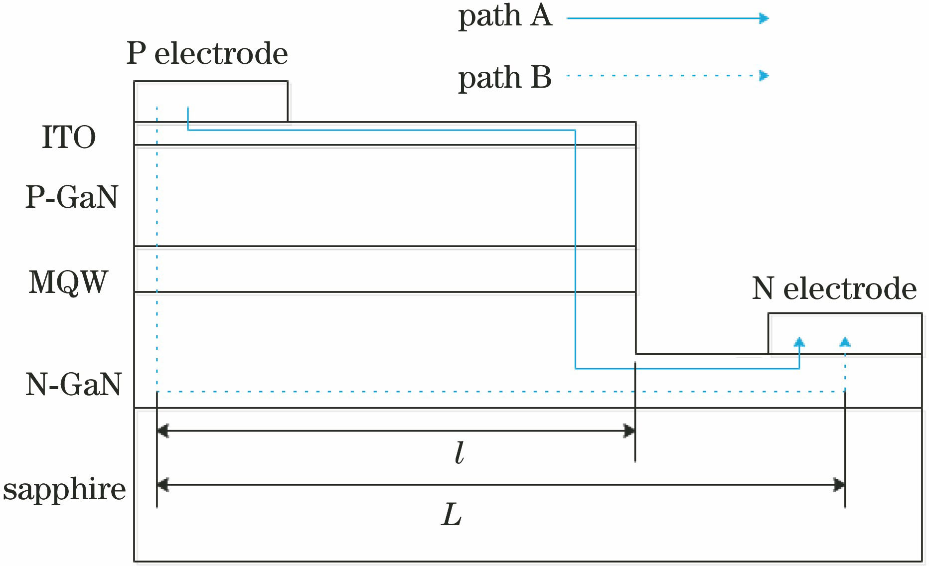
    Fig. 1. Schematic diagram of internal current path of a GaN-based LED chip
    Three-dimensional diagram of LED chips with different electrode structures. (a) Primitive structure; (b) change N electrode structure; (c) change N electrode and offset P electrode structure; (d) change N electrode and shorten P electrode structure
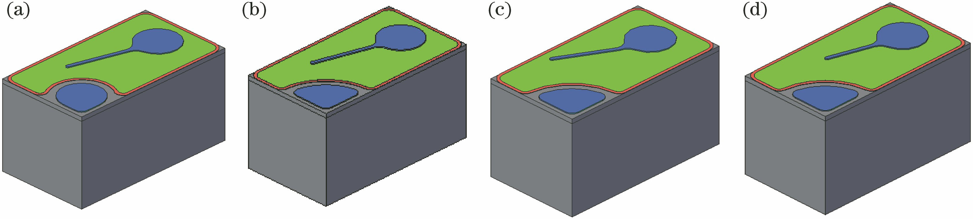
    Fig. 2. Three-dimensional diagram of LED chips with different electrode structures. (a) Primitive structure; (b) change N electrode structure; (c) change N electrode and offset P electrode structure; (d) change N electrode and shorten P electrode structure
    Current density distribution of active layer of LED chip with different electrode structures. (a) Primitive structure; (b) change N electrode structure; (c) change N electrode and offset P electrode structure; (d) change N electrode and shorten P electrode structure
    Fig. 3. Current density distribution of active layer of LED chip with different electrode structures. (a) Primitive structure; (b) change N electrode structure; (c) change N electrode and offset P electrode structure; (d) change N electrode and shorten P electrode structure
    Photo of the sample after production. (a) Primitive structure; (b) change N electrode structure; (c) change N electrode and offset P electrode structure; (d) change N electrode and shorten P electrode structure
    Fig. 4. Photo of the sample after production. (a) Primitive structure; (b) change N electrode structure; (c) change N electrode and offset P electrode structure; (d) change N electrode and shorten P electrode structure
    Near-field optical test chart of the sample. (a) Primitive structure; (b) change N electrode structure; (c) change N electrode and offset P electrode structure; (d) change N electrode and shorten P electrode structure
    Fig. 5. Near-field optical test chart of the sample. (a) Primitive structure; (b) change N electrode structure; (c) change N electrode and offset P electrode structure; (d) change N electrode and shorten P electrode structure
    I-V characteristics of four samples
    Fig. 6. I-V characteristics of four samples
    I-P characteristics of four samples
    Fig. 7. I-P characteristics of four samples
    MaterialThickness /μmResistivity /(Ω·cm)
    P-GaN0.335×10-3
    N-GaN3.005
    Electrode1.652×10-8
    Table 1. Structural parameters of COMSOL electrical model
    SampleVF /VPo /mWη /%λ /nm
    A3.0630.0049.02449.33
    B3.0631.8452.03449.36
    C3.0731.7951.86449.40
    D3.0931.9851.82449.58
    Table 2. Test data for four groups of samples
    Pengfei Chao, Yingchao Xu, Chunhui Liu, Tianyu Wu, Yangyang Li, Jianning Liu. Optimization and Preparation of GaN-Based LED Chip Electrode Structure[J]. Laser & Optoelectronics Progress, 2020, 57(7): 072301
    Download Citation