• Journal of Semiconductors
  • Vol. 40, Issue 10, 102302 (2019)
Yangjie Zhang1、2, Wentao Guo1, Di Xiong1、2, Xiaofeng Guo1, Wenyuan Liao1、2, Haifeng Liu1、2, Weihua Liu1、2, and Manqing Tan1、2
Author Affiliations
  • 1State Key Laboratory of Integrated Optoelectronics, Institute of Semiconductors, Chinese Academy of Sciences, Beijing 100083, China
  • 2Center of Materials Science and Optoelectronics Engineering, University of Chinese Academy of Sciences, Beijing 100049, China
  • show less
    DOI: 10.1088/1674-4926/40/10/102302 Cite this Article
    Yangjie Zhang, Wentao Guo, Di Xiong, Xiaofeng Guo, Wenyuan Liao, Haifeng Liu, Weihua Liu, Manqing Tan. Simulation of structural design with high coupling efficiency in external cavity semiconductor laser[J]. Journal of Semiconductors, 2019, 40(10): 102302 Copy Citation Text show less
    Schematic structure of ECSL.
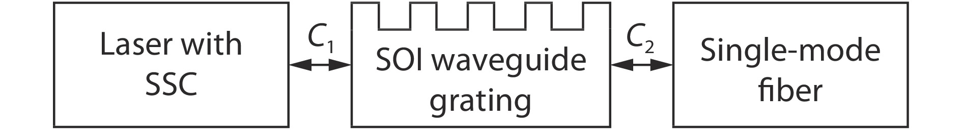
    Fig. 1. Schematic structure of ECSL.
    Schematic of the spot-size converter based on ridge waveguides.
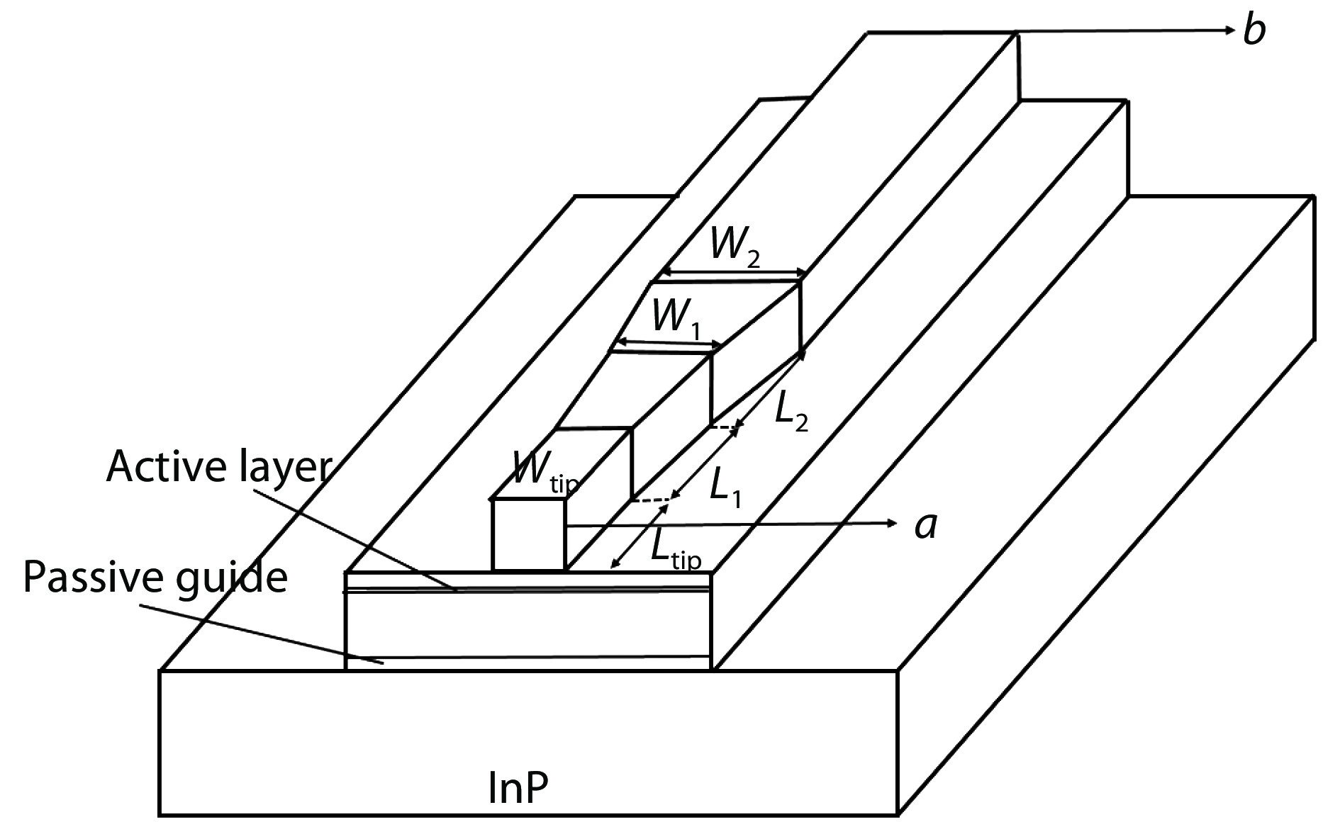
    Fig. 2. Schematic of the spot-size converter based on ridge waveguides.
    (Color online) Fundamental TE mode at the both facets of the SSC. (a) Output of TE mode at section a in Fig. 2. (b) Input of TE mode at section b in Fig. 2.
    Fig. 3. (Color online) Fundamental TE mode at the both facets of the SSC. (a) Output of TE mode at section a in Fig. 2. (b) Input of TE mode at section b in Fig. 2.
    (Color online) Coupling efficiency under different waveguide structures (Structure 1: H = 3 μm, h = 2.5 μm, W = 5 μm; Structure 2: H = 4 μm, h = 3 μm, W = 5 μm; Structure 3: H = 5 μm, h = 4 μm, W = 7 μm; Structure 4: H = 6 μm, h = 4 μm, W = 7 μm).
    Fig. 4. (Color online) Coupling efficiency under different waveguide structures (Structure 1: H = 3 μm, h = 2.5 μm, W = 5 μm; Structure 2: H = 4 μm, h = 3 μm, W = 5 μm; Structure 3: H = 5 μm, h = 4 μm, W = 7 μm; Structure 4: H = 6 μm, h = 4 μm, W = 7 μm).
    Schematic diagram of SOI ridge waveguide structure.
    Fig. 5. Schematic diagram of SOI ridge waveguide structure.
    (Color online) Total coupling efficiency C of different SOI waveguide structures. (a) H = 3 μm. (b) H = 4 μm. (c) H = 5 μm. (d) H = 6 μm.
    Fig. 6. (Color online) Total coupling efficiency C of different SOI waveguide structures. (a) H = 3 μm. (b) H = 4 μm. (c) H = 5 μm. (d) H = 6 μm.
    (Color online) Effect of coupling coefficient on linewidth characteristics of laser.
    Fig. 7. (Color online) Effect of coupling coefficient on linewidth characteristics of laser.
    (Color online) Normalized coupling power varied with the offset. (a) Vertical directions. (b) Horizontal directions (SOI waveguide of structure 4: H = 6 μm, h = 4 μm, W = 7 μm).
    Fig. 8. (Color online) Normalized coupling power varied with the offset. (a) Vertical directions. (b) Horizontal directions (SOI waveguide of structure 4: H = 6 μm, h = 4 μm, W = 7 μm).
    Yangjie Zhang, Wentao Guo, Di Xiong, Xiaofeng Guo, Wenyuan Liao, Haifeng Liu, Weihua Liu, Manqing Tan. Simulation of structural design with high coupling efficiency in external cavity semiconductor laser[J]. Journal of Semiconductors, 2019, 40(10): 102302
    Download Citation