
Yangjie Zhang, Wentao Guo, Di Xiong, Xiaofeng Guo, Wenyuan Liao, Haifeng Liu, Weihua Liu, Manqing Tan. Simulation of structural design with high coupling efficiency in external cavity semiconductor laser[J]. Journal of Semiconductors, 2019, 40(10): 102302
- Journal of Semiconductors
- Vol. 40, Issue 10, 102302 (2019)
Abstract
1. Introduction
Lasers have been widely used in the field of optical communication and optical sensing, but their application in optical communication and optical sensing is limited owing to the problem of linewidth. ECSL is applied in many fields, such as optical fiber communication, optical storage, optical gyro, coherent detection and so on, due to narrow linewidth, simple structure and convenience for largescale production. In recent years, it has become a research hotspot in the field of international optoelectronic devices[
Generally, fiber gratings, waveguide gratings, plane mirrors, etc. are applied for external cavity feedback components of ECSL[
The expansion of the near-field spot and the improvement of the coupling efficiency are realized by using the SSC. In general, reducing the linewidth of ECSL by improving coupling efficiency has been reported in the research[
Compared with fiber grating external cavity lasers, waveguide grating external cavity lasesr have better temperature stability and vibration stability[
In this paper, the coupling efficiency is calculated in detail, and the condition of single-mode is discussed. Improvement schemes including the structure of SSC and the optimizations of the structure of the SOI ridge waveguide are proposed.
2. Simulation and analysis
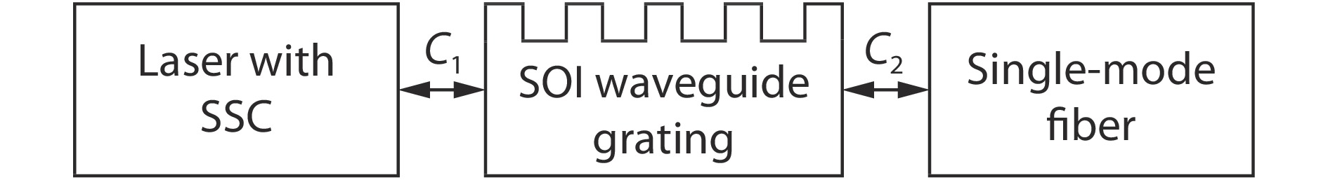
A schematic structure of ECSL is shown in Fig. 1. C1 is the coupling efficiency between laser and SOI waveguide, and C2 is the coupling efficiency between SOI waveguide and single-mode fiber. The coupling efficiency C1 and C2 were calculated by MODE Solution, which is a powerful simulation tool for planar waveguide devices. The total coupling efficiency C (C = C1 × C2) of the corresponding SOI waveguide structures are obtained.
![]()
Figure 1.Schematic structure of ECSL.
2.1. SSC model
Up to now, most SSCs were based on a buried structure with or without selective area growth. Narrow waveguides (below 0.5 μm) are used in many of these structures, which require special lithography and may be sensitive to the width of the taper tip. Recently, a new structure using resonant coupling has been presented theoretically[
![]()
Figure 2.Schematic of the spot-size converter based on ridge waveguides.
The fundamental transverse electric (TE) mode of the SSC is simulated by software[
![]()
Figure 3.(Color online) Fundamental TE mode at the both facets of the SSC. (a) Output of TE mode at section a in
MODE solution calculates the power coupling between the modes recorded by two monitors. Overlap measures the fraction of electromagnetic fields that overlap between the two modes. This is also the fraction of power from mode 2 that can propagate in mode 1 (mode 1 and mode 2 are the fundamental modes of two different waveguide structures). The overlap function is being used to estimate the efficiency C1 and C2 between the two waveguides. The overlap can be modeled as
where E1, H1 is the electric and magnetic field of mode 1; E2, H2 is the electric and magnetic field of mode 2.
Four waveguide structures are selected to calculate the coupling efficiency C1 with or without SSC. Actually, these four waveguide structures are the structures with the highest total coupling efficiency when H = 3, 4, 5, and 6 μm, respectively. Structure 1: H = 3 μm, h = 2.5 μm, W = 5 μm; Structure 2: H = 4 μm, h = 3 μm, W = 5 μm; Structure 3: H = 5 μm, h = 4 μm, W = 7 μm; Structure 4: H = 6 μm, h = 4 μm, W = 7 μm. H is the height of the inner ridge, h is the height of the outer ridge, and W is the width of the ridge. The coupling efficiency C1 under different waveguide structures is shown in Fig. 4.
![]()
Figure 4.(Color online) Coupling efficiency under different waveguide structures (Structure 1:
As can be seen from Fig. 4, the coupling efficiency C1 is greatly improved compared with the original structure without SSC except structure 1. SSC can transform the elliptical spot size of the semiconductor laser into a larger one that is close to the circular one. In addition, since the near-field spot size of the laser output end face becomes larger, the power density of the laser output surface is lowered, which effectively reduces the catastrophic damage of the laser and improves the reliability of the laser. With this method, the coupling efficiency C1 of structure 4 is increased to 93.1%, from 41.5% that of the original structure without SSC.
2.2. Optimizing the SOI waveguide structure
Fig. 5 is a schematic diagram of SOI ridge waveguide structure. n1,n2 and n3 are refractive indexes of each layer. The parameters of the SOI ridge waveguide model used in the analysis as follows. n1 = 3.5 and n2 = n3 = 1.45; fiber diameter is 8.7 μm; core index is 1.4516; cladding index is 1.4473.
![]()
Figure 5.Schematic diagram of SOI ridge waveguide structure.
In this section, the coupling efficiencies C1 and C2 of different waveguide structures are respectively calculated to obtain the total coupling efficiency C, as shown in Figs. 6(a), 6(b), 6(c) and 6(d), respectively.
![]()
Figure 6.(Color online) Total coupling efficiency
The single mode condition of the waveguide structure is not considered in the above figure, so the subsequent analysis is combined with the single mode cutoff condition. Soref[
where t = W/H, r = h/H. Therefore, the size of waveguide section is equivalent to the size of the fiber core layer, which can greatly reduce the coupling loss between waveguide and fiber.
According to the single mode condition, the critical ridge width W is theoretically calculated successively at H = 3, 4, 5, and 6 μm. Under the premise of satisfying the single mode condition, it can be seen from Fig. 6 (a) that the structure with H = 3 μm, h = 2.5 μm and W = 5 μm has the maximum total coupling efficiency, but it is still only 19.8%. The result in Fig. 6(b) confirms that the maximum total coupling efficiency (C) occurs at structure 2 (H = 4 μm, h = 3 μm, W = 5 μm), which is increased to 29.5%. The structure 3 (H = 5 μm, h = 4 μm, W = 7 μm) and structure 4 (H = 6 μm, h = 4 μm, W = 7 μm) corresponding to the maximum C are 41.2% and 48.9%, respectively. Thus, by increasing the height of the outer ridge h, the coupling efficiency between the waveguide and the optical fiber can be improved, since the mode field shape of the SOI waveguide is closer to the mode field shape of the optical fiber. However, at the same time, its overlapping mode field with the SSC is reduced. The optimum point can be determined by the above figures, which is the maximum value at a certain point in the middle of the change of the height h of the outer ridge. The total coupling efficiency of structure 4 is 48.9%. After this, the grating structure which was designed by software can be etched on the SOI waveguide.
By increasing the C0, the linewidth reduces significantly[
![]()
Figure 7.(Color online) Effect of coupling coefficient on linewidth characteristics of laser.
2.3. Alignment tolerance
Alignment tolerance is a critical aspect that has to be considered in the packaging[
![]()
Figure 8.(Color online) Normalized coupling power varied with the offset. (a) Vertical directions. (b) Horizontal directions (SOI waveguide of structure 4:
3. Conclusion
Aiming at the problems of poor spot quality, low coupling efficiency and poor stability of vibration in the waveguide grating external cavity laser, two improvement schemes are proposed. The experimental results verify the effectiveness of the new approaches investigated in this paper, which can effectively improve the coupling efficiency. In addition, we propose a scheme of SSC to optimize coupling efficiency. SOI ridge waveguide is adopted for the stability of wavelength temperature and vibration to ameliorate. The waveguide structure with the highest coupling efficiency has been determined. According to simulated results, the proposed methodology illustrated 51.6% improvement in coupling efficiency over conventional schemes.
References
[1] B Lu, F Wei, Z Zhang et al. Research on tunable local laser used in ground-to-satellite coherent laser communication. Chin Opt Lett, 13, 091402(2015).
[2] B Mroziewicz. External cavity wavelength tunable semiconductor lasers-a review. Opto-Electron Rev, 16, 347(2008).
[3]
[4] B Liu, X Tong, C Y Jiang et al. Development of stable, narrow spectral line-width, fiber delivered laser source for spin exchange optical pumping. Appl Opt, 54, 5420(2015).
[5] W Fang, Y Fei, X Zhang et al. Subkilohertz linewidth reduction of a DFB diode laser using self-injection locking with a fiber Bragg grating Fabry-Perot cavity. Opt Express, 24, 17406(2016).
[6] H K Hisham, G A Mahdiraji, A F Abas et al. Linewidth optimization in fiber grating Fabry-Perot laser. Opt Eng, 53, 026107(2014).
[7] D P Liu, n C Chen, n L Qin et al. Study on linewidth characteristics of fiber grating external cavity semiconductor laser. Semicond Optoelectron, 37, 165(2016).
[8] C H Henry. Theory of the linewidth of semiconductor lasers. IEEE J Quantum Electron, 18, 259(1982).
[9] Y J Chai, H Y Zhang, B K Zhou. Line width performance and lysis of semiconductor lasers with strong feed back external cavity. Chin J Semicond, 16, 885(1995).
[10] B W Pan, L Q Yu, u D Lu et al. 20 kHz narrow linewidth fiber Bragg grating external cavity semiconductor laser. Chin J Lasers, 42, 49(2015).
[11] M Alalusi, P Brasil, S Lee et al. Low noise planar external cavity laser for interferometric fiber optic sensors. Proc SPIE, 7316(2009).
[12] V Vusirikala, S S Saini, R E Bartolo et al. Compact mode expanders using resonant coupling between a tapered active region and an underlying coupling waveguide. IEEE Photonics Technol Lett, 10, 203(1998).
[13] H Bissessur, C Graver, O L Gouezigou et al. Ridge laser with spot-size converter in a single epitaxial step for high coupling efficiency to single-mode fibers. IEEE Photonics Technol Lett, 10, 1235(1998).
[14] T Tsuchizawa, T Watanabe, K Yamada et al. Microphotonics devices based on silicon microfabrication technology. IEEE J Sel Top Quantum Electron, 11, 232(2005).
[15] R A Soref, J Schmidthen, K Petermann. Large single-mode rib waveguide in GeSi and Si-on-SiO2. IEEE J Quantum Electron, 27, 1971(1991).
[16] A G Richman, G T Ree, F Namavar. Silicon-on-insulator optical rib waveguide loss and mode characteristics. J Lightwave Technol, 12, 1771(1994).
[17] M Sumy, S Steffen, S Ralf et al. Geometrical tolerance of optical fiber and laser diode for passive alignment using LTCC technology. German Microwave Conference, 363(2015).
[18] S Romero-Garcia, B Marzban, F Merget et al. Edge Couplers with relaxed alignment tolerance for pick-and-place hybrid integration of III–V lasers with SOI waveguides. IEEE J Sel Top Quantum Electron, 20, 369(2014).
[19] P K Shen, C T Chen, C H Chang et al. Implementation of chip-level optical interconnect with laser and photodetector using SOI-based 3-D guided-wave path. IEEE Photonics J, 6, 1(2014).

Set citation alerts for the article
Please enter your email address
© Copyright 2018-2021 | Chinese Laser Press. All Rights Reserved 沪ICP备15018463号-20