• Laser & Optoelectronics Progress
  • Vol. 57, Issue 19, 190001 (2020)
Lisha Fan1、2、3、4, Shuowen Zhang1、2、3、4, Qunli Zhang1、2、3、4, and Jianhua Yao1、2、3、4、*
Author Affiliations
  • 1College of Mechanical Engineering, Zhejiang University of Technology, Hangzhou, Zhejiang 310023, China
  • 2Institute of Laser Advanced Manufacturing, Zhejiang University of Technology, Hangzhou, Zhejiang 310023, China
  • 3Collaborative Innovation Center of High-End Laser Manufacturing Equipment (National 2011 Plan), Zhejiang University of Technology, Hangzhou, Zhejiang 310023, China
  • 4Zhejiang Provincial Engineering Research Center of High-End Equipment Laser Remanufacturing, Hangzhou, Zhejiang 310023, China
  • show less
    DOI: 10.3788/LOP57.190001 Cite this Article Set citation alerts
    Lisha Fan, Shuowen Zhang, Qunli Zhang, Jianhua Yao. Research Progress on Fabrication of One-Dimensional Well-Ordered Oxide Nanostructures by Pulsed Laser Deposition[J]. Laser & Optoelectronics Progress, 2020, 57(19): 190001 Copy Citation Text show less
    Schematic of PLD system[59]
    Fig. 1. Schematic of PLD system[59]
    Schematic of the template-assisted PLD for growing nano-ring arrays[84]
    Fig. 2. Schematic of the template-assisted PLD for growing nano-ring arrays[84]
    Schematic of catalytic-assisted PLD synthesis of nanowires[85]
    Fig. 3. Schematic of catalytic-assisted PLD synthesis of nanowires[85]
    Schematic of the growth of vertically aligned ZnO nanorods using NAPLD process[111]
    Fig. 4. Schematic of the growth of vertically aligned ZnO nanorods using NAPLD process[111]
    Schematics of the growth mechanism of one-dimensional well-ordered nanostructures by limiting surface diffusion[117]
    Fig. 5. Schematics of the growth mechanism of one-dimensional well-ordered nanostructures by limiting surface diffusion[117]
    Schematics of the perovskite-spinel composite nanostructured film by crystallization autonomous separation on {001} and {111} surfaces[126]
    Fig. 6. Schematics of the perovskite-spinel composite nanostructured film by crystallization autonomous separation on {001} and {111} surfaces[126]
    Top view and cross-sectional view SEM images of ZnO nanorods grown under three different laser influences[147]. (a-b) 4.0 J/cm2; (c-d) 1.8 J/cm2; (e-f) 1.2 J/cm2
    Fig. 7. Top view and cross-sectional view SEM images of ZnO nanorods grown under three different laser influences[147]. (a-b) 4.0 J/cm2; (c-d) 1.8 J/cm2; (e-f) 1.2 J/cm2
    Single-crystallineTiO2 nanobrushes with high energy {001} facets [119]. (a) Cross-sectional SEM images showing the nanobrush microstructure; (b) photovoltaic I/V curves of TiO2 nanobrushes, nanoparticles, and thin film
    Fig. 8. Single-crystallineTiO2 nanobrushes with high energy {001} facets [119]. (a) Cross-sectional SEM images showing the nanobrush microstructure; (b) photovoltaic I/V curves of TiO2 nanobrushes, nanoparticles, and thin film
    Hexagonal nonclose-packed TiO2 nanorod arrays[157]. (a) SEM image of the surface morphology; (b) SEM image of the cross-sectional morphology; (c) field emission I-V curve; (d) the relationship between field-enhancement factor and array period
    Fig. 9. Hexagonal nonclose-packed TiO2 nanorod arrays[157]. (a) SEM image of the surface morphology; (b) SEM image of the cross-sectional morphology; (c) field emission I-V curve; (d) the relationship between field-enhancement factor and array period
    WO3 nanorods prepared by PLD with varied W substrate temperature[168]
    Fig. 10. WO3 nanorods prepared by PLD with varied W substrate temperature[168]
    Microstructures of CoFe2O4 fabricated by surface diffusion method[120]. (a) STEM image showing the cross-sectional structure of nanobrushes; (b) atomic-resolution STEM image of the sidewall of a nanobrush; (c) STEM cross-section image showing the nanobrush/substrate interface; (d) atomic-resolution STEM image showing the nanobrush/substrate interface; (e) Fourier transform of nanobrush/substrate interface
    Fig. 11. Microstructures of CoFe2O4 fabricated by surface diffusion method[120]. (a) STEM image showing the cross-sectional structure of nanobrushes; (b) atomic-resolution STEM image of the sidewall of a nanobrush; (c) STEM cross-section image showing the nanobrush/substrate interface; (d) atomic-resolution STEM image showing the nanobrush/substrate interface; (e) Fourier transform of nanobrush/substrate interface
    SEM images of vertically aligned taper PZT nanowires arrays[179]. (a)--(g) SEM interface images of PZT nanowires prepared at varied growth temperatures; (h) the lengths of PZT nanowires and the thicknesses of PZT film in transition region as the function of growth temperature; (i) growth window of the PZT nanowires at different temperatures and pressures
    Fig. 12. SEM images of vertically aligned taper PZT nanowires arrays[179]. (a)--(g) SEM interface images of PZT nanowires prepared at varied growth temperatures; (h) the lengths of PZT nanowires and the thicknesses of PZT film in transition region as the function of growth temperature; (i) growth window of the PZT nanowires at different temperatures and pressures
    YBCO nanorods grown by PLD at different temperatures[187]. (a) 630 ℃; (b) 680 ℃
    Fig. 13. YBCO nanorods grown by PLD at different temperatures[187]. (a) 630 ℃; (b) 680 ℃
    One-dimensional CeO2/Y2O3 nanobrush superlattice[121]. (a) A STEM image showing its cross-sectional structure; (b) three-dimensional structure of one-dimensional CeO2/Y2O3 nano-superlattice reconstructed by atom probe tomography
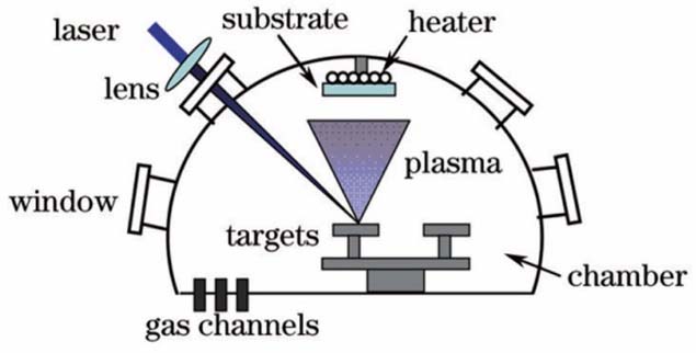
    Fig. 14. One-dimensional CeO2/Y2O3 nanobrush superlattice[121]. (a) A STEM image showing its cross-sectional structure; (b) three-dimensional structure of one-dimensional CeO2/Y2O3 nano-superlattice reconstructed by atom probe tomography
    Lisha Fan, Shuowen Zhang, Qunli Zhang, Jianhua Yao. Research Progress on Fabrication of One-Dimensional Well-Ordered Oxide Nanostructures by Pulsed Laser Deposition[J]. Laser & Optoelectronics Progress, 2020, 57(19): 190001
    Download Citation