
H. Zandipour, M. Madani. Design, modelling, and simulation of a floating gate transistor with a novel security feature[J]. Journal of Semiconductors, 2020, 41(10): 102105
- Journal of Semiconductors
- Vol. 41, Issue 10, 102105 (2020)
Abstract
1. Introduction
Non-volatile memories have many applications, including industrial, military, and general public[
In the following, a new FGT structure is presented and its C–V characteristics is modelled. Then, the trend of this model is compared to a 2D COMSOL simulation to validate the work objectives. In addition, the C–V curve obtained from the newly designed structure is compared to the conventional structure to investigate the effectiveness of this new design against SCM reverse engineering technique. Finally, an analysis of the I–V characteristics examines the feasibility of this design.
2. Proposed structures (MOPNS and MONPS)
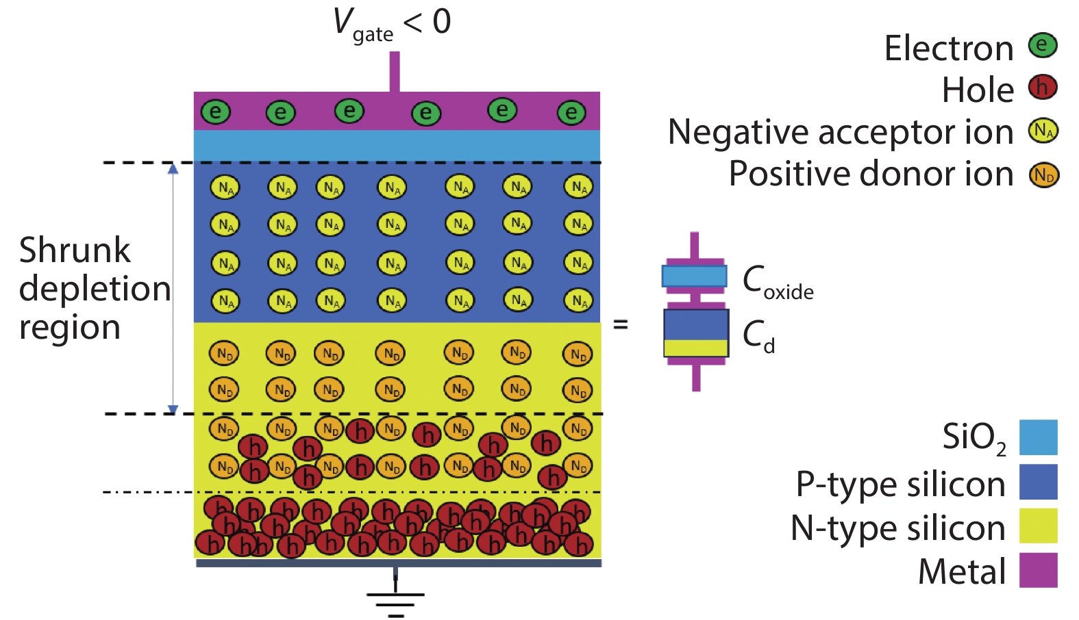
Our proposal is to form an oppositely doped compensated silicon region by ion implanting of opposite dopant in the extrinsic substrate a distance away from the SiO2–Si interface. This must be done in a way that the structure ends up with at least slightly thicker oppositely doped layer than the remaining substrate even after the back-side delayering (similar to the structure in Fig. 1). For our reference, we would like to call the structure with P-type substrate, the metal oxide P-type N-type semiconductor (MOPNS) and similarly the structure with N-type substrate, the metal oxide N-type P-type semiconductor (MONPS). From now on, the focus will be on the MOPNS, which could be easily altered to a MONPS for future applications. To start analyzing the structure, we consider the case that both regions have the same effective opposite dopant concentrations. One might say that if the substrate region depth is small enough (in tens of nm), then almost all its majority carriers will be diffused to the oppositely doped substrate (P-type region) and leave their negative ions behind; that is to say, the holes are being diffused to meet with the electrons for annihilation, and vice versa. This would happen until there are few majority carriers left in P-type region (i.e. it is depleted from its majority carries). Relatively, the N-type region will be depleted for the same depth when there is no voltage applied to the gate at thermal equilibrium because both regions have the same dopant concentration. The capacitance can also be found by treating the structure as two parallel plates capacitor by knowing the depth of this depleted region. The total capacitance, similar to an MOS, has a constant oxide capacitance (Coxide) in series with the capacitance from the depleted silicon (Cd) below the oxide layer as it is represented in Fig. 1. Furthermore, we know that in the capacitance measurement, the bottom of the device is grounded that can be considered as an abundant source of holes or electrons but these electrons and holes cannot invade the depletion region since any excess charge would unbalance the created internal electric field. However, by adding small negative or positive potential to the gate (i.e. creating an external electric field) some of those holes or electrons are eventually going to push through the depletion region and make it tighter. To clarify this explanation, the graphical representation in Fig. 1 displays a MOPNS when a small negative potential is applied to its gate. In the high frequency case, increasing the applied potential of the gate causes this depletion region to shrink to a minimum value, which causes the capacitance to go up to a certain point. Since there is not enough time for the thermal generation of electrons or hole, the depletion region stands still. However, in the case of low frequency, the depleted region vanishes completely and only the oxide capacitance will be involved.
![]()
Figure 1.(Color online) A MOPNS under the influence of small negative voltage applied to its gate.
From the energy band diagram point of view, one might say that there will be an imposed potential over the oxide and the semiconductor when a voltage is applied to the gate. By considering the energy band diagram, this applied potential to the semiconductor would cause band bending (upward or downward depending on the polarities of the applied voltage) close to the oxide interface. For example, an upward band bending can be shown in the Fig. 2 when a negative potential is applied to the gate of a MOPNS.
![]()
Figure 2.(Color online) The upward band bending in energy band diagram when a small negative voltage is applied to the gate of a MOPNS.
By finding the depletion region’s depth, we will be able to model the device capacitance. To reach this goal, one should start by finding the electric field. It is worth mentioning the boundary condition that assumes the electric field to be zero outside of the depleted N-type region (
![]()
Figure 3.(Color online) Graphical representation of charge density, electric field and electric potential of a MOPNS.
The electric fields in both P-type (E1) and N-type (E2) regions can be found by integrating the charge density divided by the permittivity over each region (from Gauss's law). The electric field in each region can be found as:
where q is the elementary charge,
By having the electric field, one can calculate the electric potential over the semiconductor by integrating the electric field (with a negative sign) over both regions. So, the potential drop over the semiconductor can be calculated as:
where
We also know that the applied voltage to the gate (
One can easily obtain the
Now, one may calculate the
3. Results and comparison
To validate the driven formula, a 2D COMSOL simulation has been done on a MOPNS with the same dimensions as Fig. 4 to find the low (0.1 Hz) and high (109 Hz) frequency capacitance of the device versus the offset voltage applied to the gate with the work function of 4 V. As can be seen in Fig. 4, the bottom N-type region has the donor concentration of
![]()
Figure 4.(Color online) Donor concentration of a simulated MOPNS.
![]()
Figure 5.(Color online) Comparison between the extracted model and simulation results (for HF and LF) of normalized
To see how effective this design could be, a comparison between the high frequency C–V behaviours of an FG MOPNS and a traditional P-type FG MOS is depicted in the Fig. 6, which may also represent the outcome of the SCM technique. Both structures have the same structure size as Fig. 7 and also equal dopant concentrations as
![]()
Figure 6.(Color online) Comparison of HF
![]()
Figure 7.(Color online) Donor concentration of a MOPNS transistor.
To expand our investigation on the effect of the added layer, a comparison between an FG MOPNS with three different dopant concentrations of oppositely doped region (N-type) is done. Fig. 8 shows this comparison between three different donor concentrations of
![]()
Figure 8.(Color online) Comparison of HF
Even though the obtained results from the C–V curve seems desirable, it is important to have a practical device otherwise the design would be useless. To have a functional device, the structure needs to have a similar functionality (i.e. I–V characteristic) as a simple P-type FG MOS. To take this into account, normalized I–V characteristics of an FG MOPNS transistor and a P-type FG MOS transistor are depicted in Fig. 9. Both structures have the same size as Fig. 7. The FG MOPNS transistor have the dopant concentrations of
![]()
Figure 9.(Color online) Comparison between
This comparison shows an insignificant change in the I–V characteristics. That is to say, the desirable shift in the I–V characteristic is clearly observed when the FG is charged, which supports the idea that our FG MOPNS transistor has similar functionality as a traditional P-type FG MOS transistor.
4. Conclusion
In this work, we have presented a new FG transistor design structure that can be used to safeguard the states of FG transistors against a vigorous reverse engineering skim, SCM. To develop a more efficient design, we represented the idea of implanting an oppositely doped region at the bottom of the silicon substrate, close to the oxide interface beyond delayering limit without changing the transistor normal operation characteristics. A simple model was extracted to describe the new design’s C–V characteristic, which was then validated by the designated simulation. Later, a comparison between an FG MOPNS and a traditional P-type FG MOS showed a significant drop in the maximum measured capacitance, as well as a huge drop in the difference between maximum and minimum measured capacitance, when both the implanted region and the substrate have the same dopant concentration. Furthermore, it was observed that the dopant of this implanted region has a great influence on the C–V characteristic of the device. Our results have shown to have the same trend as a P-type FG MOS when the dopant concentration of the implanted layer is very low compared to the substrate. Meanwhile, the behavior observed to be similar to an N-type FG MOS when the dopant concentration of the implanted layer is very high compared to the substrate. In addition, our results show that the new device can be tuned to have different C–V characteristics. This adds to the complexity of choosing the right device with the right C–V characteristic, which may be considered as a security feature. Manufacturers may also take advantage of this result to obfuscate the stored data on their chip by implanting this layer at arbitrary spots with equal or greater dopant concentration than the substrate. Finally, the I–V characteristic of an FG MOPNS transistor were compared to an FG MOS transistor and very little difference in behavior was observed. This indicates that the proposed structure has the same functionality as a traditional FG MOS transistor. One might say that the attained results are encouraging and they point to a potentially practical design. It is worth noting that this design is not costly because the required ion implantation process is already implemented in the bipolar transistor fabrication to increase the collector’s efficiency.
References
[1] O Fujita, Y Amemiya. A floating-gate analog memory device for neural networks. IEEE Trans Electron Devices, 40, 2029(1993).
[2] G Wang, X Liu, W Wang. Solution processed organic transistor nonvolatile memory with a floating-gate of carbon nanotubes. IEEE Electron Device Lett, 39, 111(2018).
[3] X Jia, P Feng, S Zhang et al. An ultra-low-power area-efficient non-volatile memory in a 0.18
[4] J Lee, Y Jeong, H Jeong et al. Fabrication and characterization of a new EEPROM cell with spacer select transistor. IEEE Electron Device Lett, 26, 569(2005).
[5] L Fang, W Kong, J Gu et al. A novel symmetrical split-gate structure for 2-bit per cell flash memory. J Semicond, 35, 074008(2014).
[6] P Cacharelis, E Fong, E Torgerson et al. A single transistor electrically alterable cell. IEEE Electron Device Lett, 6, 519(1985).
[7] D Dimaria, K Demeyer, D Dong. Electrically-alterable memory using a dual electron injector structure. IEEE Electron Device Lett, 1, 179(1980).
[8] J Wu, L Q Zhang, Y Yao et al. Investigation of dynamic threshold voltage behavior in semi-floating gate transistor for normally-off AlGaN/GaN HEMT. IEEE J Electron Devices Soc, 5, 117(2017).
[9] Y M Kim, S J Kim, J S Lee. Organic-transistor-based nano-floating-gate memory devices having multistack charge-trapping layers. IEEE Electron Device Lett, 31, 503(2010).
[10] H Schauer, L V Tran, L Smith. A high-density, high-performance EEPROM cell. IEEE Trans Electron Devices, 29, 1178(1982).
[11] A Kolodny, S Nieh, B Eitan et al. Analysis and modeling of floating-gate EEPROM cells. IEEE Trans Electron Devices, 33, 835(1986).
[12] M Holler, M Guizar-Sicairos, E H R Tsai et al. High-resolution non-destructive three-dimensional imaging of integrated circuits. Nature, 543, 402(2017).
[13] S E Quadir, J Chen, D Forte et al. A survey on chip to system reverse engineering ACM. J Emerg Technol Comput Syst, 13, 1(2016).
[14] A K Henning, T Hochwitz, J Slinkman et al. Two-dimensional surface dopant profiling in silicon using scanning Kelvin probe microscopy. J Appl Phys, 77, 1888(1995).
[15] L Bidani, O Baharav, M Sinvani et al. Usage of laser timing probe for sensing of programmed charges in EEPROM devices. IEEE Trans Device Mater Reliab, 14, 304(2014).
[16]
[17] C Denardi, R Desplats, P Perdu et al. Descrambling and data reading techniques for flash-EEPROM memories. Application smart cards. Microelectron Reliab, 46, 1569(2006).


Set citation alerts for the article
Please enter your email address

© Copyright 2018-2021 | Chinese Laser Press. All Rights Reserved 沪ICP备15018463号-20