• Journal of Semiconductors
  • Vol. 43, Issue 11, 113101 (2022)
Lulu Guan1, Xingyu Li1, Dongchen Che2, Kaidong Xu1、2, and Shiwei Zhuang1、*
Author Affiliations
  • 1School of Physics and Electronic Engineering, Jiangsu Normal University, Xuzhou 221116, China
  • 2Jiangsu Leuven Instruments Co. Ltd, Xuzhou 221300, China
  • show less
    DOI: 10.1088/1674-4926/43/11/113101 Cite this Article
    Lulu Guan, Xingyu Li, Dongchen Che, Kaidong Xu, Shiwei Zhuang. Plasma atomic layer etching of GaN/AlGaN materials and application: An overview[J]. Journal of Semiconductors, 2022, 43(11): 113101 Copy Citation Text show less
    (Color online) Schematic of (a) isotropic etching and (b) anisotropic etching.
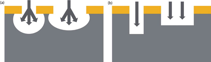
    Fig. 1. (Color online) Schematic of (a) isotropic etching and (b) anisotropic etching.
    (Color online) Schematic of one plasma ALE cycle generic concept.
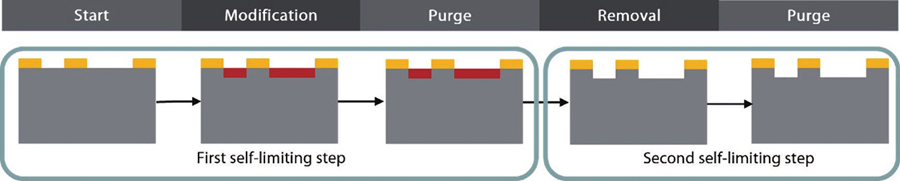
    Fig. 2. (Color online) Schematic of one plasma ALE cycle generic concept.
    (Color online) (a) Measured data of etching rate per cycle for a fixed BCl3 plasma time per cycle and varying oxygen plasma time per cycle. (b) The linear behavior of the plasma ALE etching rate versus the number of plasma ALE cycles[64].
    Fig. 3. (Color online) (a) Measured data of etching rate per cycle for a fixed BCl3 plasma time per cycle and varying oxygen plasma time per cycle. (b) The linear behavior of the plasma ALE etching rate versus the number of plasma ALE cycles[64].
    (Color online) Schematic of mechanism of GaN O2–BCl3 plasma ALE.
    Fig. 4. (Color online) Schematic of mechanism of GaN O2–BCl3 plasma ALE.
    (Color online) Schematic of one Cl2/BCl3-inert gas plasma ALE cycle generic concept.
    Fig. 5. (Color online) Schematic of one Cl2/BCl3-inert gas plasma ALE cycle generic concept.
    EPC of GaN as a function of bias voltage[52].
    Fig. 6. EPC of GaN as a function of bias voltage[52].
    (Color online) GaN plasma ALE process and initial parameters[78].
    Fig. 7. (Color online) GaN plasma ALE process and initial parameters[78].
    EPC as a function of the absolute value of the self-bias potentialVDC by varying RF bias for (a) an removal by Ar plasma with an RF source set at 100 W (full triangle) and 120 W (empty triangle) and (b) an activation by Kr plasma for an RF source set at 100 W (full square) and 120 W (empty square)[80].
    Fig. 8. EPC as a function of the absolute value of the self-bias potentialVDC by varying RF bias for (a) an removal by Ar plasma with an RF source set at 100 W (full triangle) and 120 W (empty triangle) and (b) an activation by Kr plasma for an RF source set at 100 W (full square) and 120 W (empty square)[80].
    (Color online) (a) Post-etching GaN layer thickness for the unetched reference, after the chlorination step only, after He or Ar plasma only and after full He or Ar plasma ALE (60 cycles) and (b) energy scan for Ar and He ALE processes[83].
    Fig. 9. (Color online) (a) Post-etching GaN layer thickness for the unetched reference, after the chlorination step only, after He or Ar plasma only and after full He or Ar plasma ALE (60 cycles) and (b) energy scan for Ar and He ALE processes[83].
    (Color online) The mechanism of Cl2–He plasma ALE process.
    Fig. 10. (Color online) The mechanism of Cl2–He plasma ALE process.
    Lulu Guan, Xingyu Li, Dongchen Che, Kaidong Xu, Shiwei Zhuang. Plasma atomic layer etching of GaN/AlGaN materials and application: An overview[J]. Journal of Semiconductors, 2022, 43(11): 113101
    Download Citation