Abstract
With the development of the third generation of semiconductor devices, it is essential to achieve precise etching of gallium nitride (GaN) materials that is close to the atomic level. Compared with the traditional wet etching and continuous plasma etching, plasma atomic layer etching (ALE) of GaN has the advantages of self-limiting etching, high selectivity to other materials, and smooth etched surface. In this paper the basic properties and applications of GaN are presented. It also presents the various etching methods of GaN. GaN plasma ALE systems are reviewed, and their similarities and differences are compared. In addition, the industrial application of GaN plasma ALE is outlined.With the development of the third generation of semiconductor devices, it is essential to achieve precise etching of gallium nitride (GaN) materials that is close to the atomic level. Compared with the traditional wet etching and continuous plasma etching, plasma atomic layer etching (ALE) of GaN has the advantages of self-limiting etching, high selectivity to other materials, and smooth etched surface. In this paper the basic properties and applications of GaN are presented. It also presents the various etching methods of GaN. GaN plasma ALE systems are reviewed, and their similarities and differences are compared. In addition, the industrial application of GaN plasma ALE is outlined.Introduction
Micro- and nano-fabrication techniques have been given an increasingly important role in modern manufacturing[1]. The development semiconductor industry has gone through three stages, which can be divided by materials[2]. Silicon (Si) and germanium (Ge) are regarded as the first generation of semiconductors. Gallium arsenide (GaAs) and indium phosphide (InP) have been widely accepted as the second generation of semiconductor materials[3,4]. Nowadays, the third generation of semiconductors are known as wide band-gap semiconductor materials, referring to materials with band gap greater than 2.3 eV[5]. Typically, the third-generation materials are represented by gallium nitride (GaN)[6], silicon carbide (SiC)[7], and so on[8,9]. The band gap of GaN (3.45 eV), for example, is almost three times superior to that of Si (1.2 eV) and GaAs (1.45 eV)[10-12]. GaN-based HEMTs (high electron mobility transistors), such as AlGaN/GaN[13] and InAlGaN/GaN[14], have strong spontaneous polarization and piezoelectric polarization effects[15]; advantages such as high power, high temperature[16], high breakdown voltage, high current density[17], high frequency characteristics[18]; and thus are emerging in a broad range of applications in power electronics[19], radio frequency[20], optoelectronics[21], and many other fields[22].
Low-damage etching is a crucial step in the fabrication process of GaN HEMT because etching damage might cause device oscillation or overshoot, which further causes device destruction[23]. Generally, etching is a continuous and simultaneous process[24]. The continuous process is conducive to a high etching rate; however, etching morphology has poor controllability. The most critical factor affecting device performance is the surface roughness and controllable etching depth. In this context, atomic layer etching (ALE) is a technique that uses self-limiting reactions to remove an atomic layer of materials. The concept of removing a single atomic layer from a solid surface was first proposed in a patent by Yoder, who outlined a method for "atomic layer etching" of crystalline diamond[25]. Since then, ALE has drawn attention in fields that require precise etching, and has been regarded as the most promising strategy to achieve atomic-level etching controllability with low-damage[26-29]. However, there has not yet been a systemic review focus on plasma ALE of GaN materials. In this context, the efforts with respect to GaN plasma ALE will first be briefly reviewed. Next, an attempt is made to discuss the etching mechanism and its principle. Then, we introduce the etching results brought by different GaN plasma ALE systems. Finally, the conclusion and a brief prospect for its industrial application are presented.
Etching of GaN/AlGaN
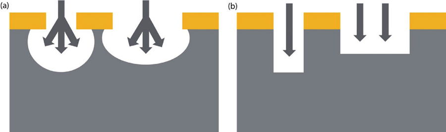
Etching is a crucial step that is used in nanofabrication to remove substrate or excess material from the surface by chemical or physical methods. Historically, patterns were etched by wet chemical methods, which proceed in all directions with roughly the same rate. Thus, the application of wet methods for GaN is mostly limited to patterns with large features size (Fig. 1 (a))[30]. For example, the isotropic etching of GaN and AlGaN material using basic solutions (KOH, NaOH etc.)[31-33].

Figure 1.(Color online) Schematic of (a) isotropic etching and (b) anisotropic etching.
With the shrinking of feature size, plasma dry etching was introduced in the 1980s and has attracted intensive attention for precise pattern conversion. Plasma dry etching proceeds by either chemical, physical or physicochemical etching to achieve high etching rate[24]. Among different plasma etching processes, physical and physicochemical plasma dry etching can realize anisotropic etching (Fig. 1 (b))[34]; for example, ICP etching can achieve higher plasma density, wider plasma uniformity, and obtain a high etching rate while maintaining better etching morphology, which makes it easier to achieve mass production with low operating costs[35].
As the feature size of semiconductor devices further shrinks to the sub-10 nm scale, the existing etching technologies are gradually unable to meet the requirements of micro-size etching controllability (precise etching depth, profile etc.). In this context, ALE methods, including plasma and thermal ALE[24,36-38], are emerging to break through the limitations of the mentioned continuous etching methods and realize atomic level etching precision by removing material layer-by-layer etching.
ALE was termed by Yoder in 1988 and has been developed for more than 30 years to achieve precise etching[25]. The generic principle behind ALE is to break down an etching process into two successive controlled, self-limiting surface reaction steps that begin with surface modification and are followed by the removal of the modified layer, as shown inFig. 2. At the first step, a self-limited reaction takes place between the exposed layer and the modification gas. After purging off the excess modification gas, the removal step takes away the modified layer and refreshes the underlying bulk material for the next cycle. This cyclic etching process can result in a uniform and smooth surface. The modification is isotropic, while the directionality of the energetic ions and neutral atoms in plasma provide the anisotropic etching that is needed to fabricate high aspect ratio features. Therefore, plasma ALE is more suitable for GaN-based HEMTs fabrication, compared to thermal ALE[39-41]. Until now, plasma ALE has been demonstrated over 20 materials, such as Ge[42], Si[43], GaAs[44], InP[45], graphene[46], polymer[47], Si3N4[48], SiO2[49], TiO2[50], Al2O3[51], GaN[52].
Figure 2.(Color online) Schematic of one plasma ALE cycle generic concept.
Plasma atomic layer etching of GaN/AlGaN
GaN HEMTs are inherently normally-on as long as an AlGaN/GaN heterostructure is formed[53]. For commercial applications (reduced energy loss, positive gate threshold tension, etc.), enhancement mode (normally-off operation) is desirable for its reduced energy loss and positive gate threshold tension[22]. Therefore, several approaches have been proposed to make normally-off GaN HEMTs such as gate recess[54], fluorine implantation[55], p-GaN gate[56], ultra-thin barrier layer structure[57], cascode structure[58], and so on. Among the manufacturing methods for GaN enhancement mode devices, gate recess etching may be the most promising technique. Recess etching is critical because it determines the threshold voltage and leakage current of the HEMT. The high etching rate of continuous etching makes it less controllable in recess etching. Therefore, plasma ALE is more suitable for recess etching. This section will introduce different plasma ALE etching systems in GaN/AlGaN transistor fabrication process.
O2–BCl3 system
It has been demonstrated that a thin oxidized layer on an AlGaN surface can be created by low power N2O or O2 plasma[59]. Subsequently, the oxidized layer can be removed from the intrinsic material with either Brønsted acid (HCl[60], BOE solution[61]) or Lewis acid (BCl3 plasma[62]). The oxidized AlGaN/GaN layer has a self-limiting depth with time and a linear relationship with plasma power[63]. Since pure BC13 was found to be virtually ineffective for etching GaN[62], the plasma ALE with O2–BCl3 system shows high controllability and can obtain a more uniform, low damage etching process.
In 2010, Burnhamet al. studied the O2–BCl3 plasma ALE for GaN HEMT devices fabrication[64,65]. The oxidation of GaN surface by low power O2 plasma is self-limiting, the depth of the oxidized layer increases from 1.4 to 2.5 nm in 15 s and remains constant with higher O2 plasma exposure time (Fig. 3(a)). Therefore, this self-limiting etch technique leads to improved repeatability, uniformity, and linearity across the whole wafer compared to the fluorine-treatment process[66]. The linearity experiment showed that the etching rate of GaN plasma ALE has a linear relationship with the number of cycles (Fig. 3(b)), which reflects the controllability of O2–BCl3 system GaN plasma ALE.
Figure 3.(Color online) (a) Measured data of etching rate per cycle for a fixed BCl3 plasma time per cycle and varying oxygen plasma time per cycle. (b) The linear behavior of the plasma ALE etching rate versus the number of plasma ALE cycles[64].
To understand the etching mechanism during the O2–BCl3 ALE process, complementary X-ray Photoelectron Spectroscope (XPS) analyses have been performed by Rouxet al.[67]. After the oxidation step, oxidation of the GaN surface is observed because XPS shows a huge increase of O–Ga bonds and dramatically decrease of N–Ga and N–O bonds. This indicates the combination of oxygen and removal of nitrogen from the gallium rich surface. The self-limiting character of the oxidation step was also monitored and verified by XPS, and all spectra reach a saturation level after 30 s O2 treatment. After BCl3 plasma exposure, oxygen concentration decreases to around 8.8% and stays stable with increasing treatment time. Gallium oxide layer can be selectively removed by BCl3 plasma[68]. At the same time Cl–B and B–N peaks are newly detected around 198.7 ± 0.09 and 189.18 ± 0.09 eV, respectively. It is assumed that the BCl3 plasma is deposited on the non-oxidized GaN surface. Therefore, the O2–BCl3 ALE is a low damage process. BCl3 has a strong affinity for oxygen. BCl3 ions react with the oxygen of gallium oxide to form B3Cl3O3, an inert gas, which can be pumped away. Gallium reacts with chlorine to form volatile GaCl3. Chloride ions can etch GaN and provide energy for sputtering GaCl3 from the surface. The remaining nitrogen reacts to produce volatile compounds N2 and NCl3.Fig. 4 shows the mechanism of GaN O2–BCl3 plasma ALE. Hwanget al. studied some other properties of etched GaN using O2–BCl3 plasma ALE[69].
Figure 4.(Color online) Schematic of mechanism of GaN O2–BCl3 plasma ALE.
Compared with devices fabricated using traditional fluorine plasma treatment process, such as CF4 plasma, the devices with O2–BCl3 ALE process result in higher uniformity of threshold voltage (±150 mV, σ = 63 mV), higher peak transconductance (246 mS/mm atVgs = 1 V), improved current collapse (34%) and breakdown voltage (>1100 V), and relative low leakage current (10µA/mm,Vds = 1100 V)[64,65]. These improvements in electrical performance show the great potential of the O2–BCl3 plasma ALE technique in AlGaN/GaN MOS-HEMTs fabrication for power switching applications. With this atomic level-controlled low-damage gate recess process, normally off AlGaN/GaN MOS-HEMTs have been fabricated by Huet al. in 2018[70]. The resulting devices exhibit low on-resistance (10.1 Ω∙mm) with a threshold voltage over 2.2 V, and a saturation current of 518 mA/mm. In the meantime, a high breakdown voltage of 1456 V with a low off-state current density (1μA/mm) has been also achieved.
It is of note that the application of O2–BCl3 is not limited in AlGaN/GaN HEMTs fabrication. Recently, Duet al. demonstrated the application of O2–BCl3 ALE technique for InAlN/GaN heteroepitaxy in detail[71]. The atomic force microscopy results show improved surface roughness (0.28 nm) compared to that of the as-grown InAlN surface (0.45 nm) and the surface obtained from widely used BCl3 plasma etching (0.69 nm).
Chlorinate-inert gas system
Another well-known system of GaN plasma ALE is to chlorinate the surface through chemical adsorption, and then sputter the "chlorination layer" with inert gas plasma. Since chlorine has a high affinity for trivalent metal atoms, chlorine plasma can be utilized in GaN etching to form highly volatile gallium chloride products. When the surface of wurtzite GaN (0001) is exposed to Cl2 for chlorination, chlorine preferentially reacts with Ga to form gallium chloride. Gallium chloride is volatile under vacuum[35], which makes it easier to remove. The study of Harafujietal. showed that when the unmodified GaN is bombarded with Ar plasma[72], compared with Ga, Ar preferentially etches N. This happens because the energy threshold of sputtered N is smaller than that of Ga. By introducing chlorine gas to modify the GaN surface, the threshold of Ga sputtering can be lowered. This characteristic has more profound significance in low-power environments. By forming a chlorinated surface to decrease inert gas plasma energy, plasma induced bombardments are effectively suppressed. Inert gas bombardment of the chloride layer can achieve anisotropic etching. A schematic of one Cl2/BCl3-inert gas plasma ALE cycle generic concept is given inFig. 5.
Figure 5.(Color online) Schematic of one Cl2/BCl3-inert gas plasma ALE cycle generic concept.
In 2017, a different ALE process was developed for GaN/AlGaN HEMTs by Ohbaet al.[73]. In this new ALE process the GaN surface is modified using chlorination (e.g., Cl2 plasma) instead of oxidation, and the modified layer was removed by Ar plasma, which realized anisotropic etching and made the patterned features directional[52]. A purge cleaning step is added between the modification step and the removal step, so as to minimize the interaction between the two steps and ensure the reliability of the experiment. The etch per cycle (EPC) was 0.4 nm/cycle with ultra-smooth surface, which is promising for use in next-generation power devices. The root-mean-square surface roughness (0.6 nm), which was improved from an as-grown surface roughness (0.8 nm). Measurable surface roughness (1.8 nm) was observed when only Cl2 is engaged in chlorination step, which was caused by the oxygen contamination in the chamber and can be suppress to 0.3 nm by adding BCl3 to the chlorination step, since BCl3 can scavenge oxidized materials on the GaN surface. For a fixed Ar step time of 5 s,Fig. 6 shows the relationship between the GaN EPC and the bias voltage. The EPC is almost constant at bias voltage 50–100 V (region II), as the bias voltage can provide sufficient sputtering energy for GaCl3 removal, while the energy does not reach the physical sputtering threshold and will not lead to pure sputtering etching.
Figure 6.EPC of GaN as a function of bias voltage[52].
The synergistic effect is defined as a percentage relative to the total amount of material removed per cycle, which is an essential parameter reflecting the controllability and accuracy in ALE process[74]. In the optimized ALE window, etching caused by Cl2 chlorination is negligible, and that caused by argon sputtering is 0.05 nm. Therefore, the synergy of Cl2–Ar plasma ALE of GaN is about 86.5%. In addition, Aroulandaet al. reported the Cl2/Ar modified and Ar removal system, and obtained an etching rate close to the molecular layer per cycle: 0.17 nm/cycle[75]. However, the synergy of this system is not ideal due to the Ar ion bombardments.
In 2019, Fukumizuet al. found that the etching damage of AlGaN/GaN stacked layers caused by Cl2–Ar plasma ALE was higher than that by Cl2/Ar RIE[76]. Generally, etching damage caused by plasma is mainly caused by radicals, ions and photons. The energy of radicals is low, so they can only cause surface penetration during the etching process. It has been shown that the penetration depth of Ar ions is about 0.5 nm[77]. By researching the optical emissions of the Cl2 plasma in the modification step, the author found that photons could penetrate into not only the AlGaN but also the GaN beneath the AlGaN. Therefore, the plasma-induced damage in the unetched GaN film was attributed to UV photons but not to ions and radicals. The UV photons are mainly produced by Cl2 plasma. The author proposed using Cl2 gas instead of Cl2 plasma for modification. The results showed that the photon damage obtained by using Cl2 gas ALE is less than that of Cl2 plasma ALE. However, the etching damage is still greater than RIE. Owing to plasma ALE long process time, the UV photon-induced damage is serious. In general, the GaN surface roughness after RIE increases with etching depth. Although the UV photon-induced damage caused by Cl2–Ar plasma ALE is relatively serious, the most critical factor affecting device performance is the surface roughness and controllable etching depth. Plasma ALE is still the most suitable precision etching technique for power devices.
During their study of the Cl2–Ar plasma ALE process, Kauppinen also proved that the etching depth increases linearly with the number of cycles, which shows the etching rate is almost stable[78]. Interestingly, adding purge step between the modification and removal steps has a significant impact on the etching ratio, which is probably caused by the residual chlorine (Fig. 7). When the purge time increased, the etching rate gradually decreased and reached an equilibrium state when the time of 20 s, indicating completely removal of remaining Cl2 which needs at least 20 s. The shorter the purge time, more Cl2 remains which etches more GaN at the Ar plasma step. While the remaining Cl2 was totally removed, the etching rate will not change when other variables are constant.
Figure 7.(Color online) GaN plasma ALE process and initial parameters[78].
The purge step between the modification and removal steps has an impact on the etching results. The effect of residual chlorine on the etching rate was explored by changing the purge time. As the purge time increased, the etching rate gradually decreased, and reached an equilibrium state when the time of 20 s. This happens because too short a time (less than 20 s) is not enough to completely purge the remaining Cl2 in the chamber (i.e., the shorter the purge time, more Cl2 will remain). When RF power is added for etching, the remaining Cl2 will generate plasma to increase the etching depth. When the purge time is long enough (more than 20 s), the remaining Cl2 will be purged, so that the etching rate will not change when other variables are constant.
The plasma ALE gate recess could be a compelling technique in the fabrication of AlGaN/GaN heterostructure-based HEMTs. In 2020, Zhangetal. developed the Cl2–Ar plasma ALE to gate recess for fabrication of T-gate millimeter-wave AlGaN/GaN HEMTs[79]. The result showed that the suppressed etching damages can be realized by pulsed current–voltage characterization. Compared with conventional gate recess process, the ALE-recessed HEMTs exhibit a high power-added-efficiency (PAE) at 40 GHz (43.6%), which is about 12.8% higher. That happens because the reverse gate leakage current in the ALE-recessed HEMTs is reduced by more than two orders of magnitude, contributing to a high breakdown voltage (127 V) with a gate-drain separation (LGD) of 1.5μm.
Other inert gas plasma, such as Kr and He, have also been studied for removal step. In 2020, Mannequinet al. reported the removal of Chlorinated layer with Kr plasma[80]. In their study, RF bias was only added in the modified layer removal step. The etching rate increases with the RF bias as the ion energy sputtering on the GaN surface increases with the bias voltage. By studying of both Ar and Kr plasma in the modified layer removal step, it has been verified that the modification layer removal with Kr plasma has a larger ALE window (Fig. 8). According to the approach developed by Berryet al.[81], experimental results qualitatively confirmed the strong dependence of the plasma ALE window on the ion mass of the removed species. In addition, different energy distribution of Ar ions and Kr ions may be one of the reasons to explain the different window. Kawakamiet al. compared the damage of GaN etched by Kr and Ar plasma[82]. Kr plasma etching can obtain smoother surfaces, thinner etching depths, and preferentially etch Ga compared to Ar plasma. But the explanation of its mechanism has not been clear so far. It is worth noting that under this research system, the obtained synergy is poor (62%), which is due to the Kr plasma etching of unmodified GaN layer.
Figure 8.EPC as a function of the absolute value of the self-bias potentialVDC by varying RF bias for (a) an removal by Ar plasma with an RF source set at 100 W (full triangle) and 120 W (empty triangle) and (b) an activation by Kr plasma for an RF source set at 100 W (full square) and 120 W (empty square)[80].
To increase the synergy of chlorination-remove ALE process, suppressing the bombardment at the removal step is necessary. Therefore, helium is more preferred to be engaged as a removal gas because it has less molecular weight. In 2021, Ruelet al. compared the etching results using Ar plasma and He plasma for chlorinated layer removal in detail[83]. As is depicted inFig. 9(a), no GaN etching is detected when Cl2 chlorination is used alone, and the etching rate is minimal when He or Ar step only. The synergy Cl2–Ar plasma ALE is 92.5%, while that of Cl2–He plasma ALE can reach as high as 99%.
Figure 9.(Color online) (a) Post-etching GaN layer thickness for the unetched reference, after the chlorination step only, after He or Ar plasma only and after full He or Ar plasma ALE (60 cycles) and (b) energy scan for Ar and He ALE processes[83].
The mechanism of Cl2–He plasma ALE process is shown inFig. 10. During the first cycle, Cl2 plasma chlorinates the surface through chemical adsorption, and then the "chlorination layer" is sputtered with He plasma. The small mass and size of He ions allow them to penetrate deep into the surface of GaN and form a penetration layer. As a result, a deeper Cl diffusion layer generates after Cl2 plasma chlorination in the second cycle. The EPC of using He as removal plasma is much higher than that using Ar. Since no etching is detected on unchlorinated GaN surface with helium plasma, the higher EPC can be attributed to He ions penetration. Deeper helium penetration and diffusion of Cl ions explain the high etching rate of Cl2–He plasma ALE. As is shown inFig. 9(b), comparing to the system with Ar plasma, the etching rate window with He plasma shifted to lower bias voltage side because of He ions penetration (region II).
Figure 10.(Color online) The mechanism of Cl2–He plasma ALE process.
By comparing theRsheet after IBE etching, Cl2–Ar plasma ALE and Cl2–He plasma ALE, results showed that the relative sheet resistance (Rsheet) of 2DEG channel after Cl2–He plasma ALE process increases sharply. This is related to the penetration of He ions into the GaN surface. N2 annealing can significantly reduceRsheet, that is, N2 annealing can repair the damage caused by He ion penetration[84].
Atomic layer etching of GaN using Cl2 and inert gas plasma has been researched. Compared with Cl2–Ar plasma ALE, Cl2–Kr plasma ALE can obtain a smoother etched surface, but the synergy obtained is poor. Cl2–He plasma ALE has good synergy. However, due to the penetration of He ions, the electrical damage caused by etching is relatively large. The purpose of GaN plasma ALE process is to achieve a more controllable etched surface with less damage. It is therefore necessary and far-reaching to verify the other parameters to reduce electrical damage to obtain better device performance.
Conclusion and prospective
So far, many systems of the GaN/AlGaN plasma ALE process have been developed. Self-limiting O2–BCl3 plasma ALE can obtain uniform threshold voltage, high peak transconductance, good current collapse, high breakdown voltage and low leakage current. This etching technique could achieve low-damage plasma etching, which provides a promising technique for gate recess etching to fabricate electronic module devices. When etching AlGaN, adding BCl3 can reduce the generation of deposits. At the same time, the formation of BCl2+ and BCl3+ heavy ions can physically bombard the surface and reduce roughness. As mentioned earlier, Cl2-inert gas plasma ALE is self-limiting both on modification and removal steps. To obtain ideal atomic-lever etching and better etching results, different removal gases have been studied. The selection of the rare gas Ar and Kr for the removal step is self-limiting, but He is not self-limiting. This is due to the small mass and size of He ions that enable them to penetrate the GaN surface. It is worth noting that when He removes the modified layer, the penetration of He ions brings greater etching damage on unmodified layer.
This article introduces the different existing GaN/AlGaN atomic layer etching systems and compares the similarities and differences of each system, which can be used as a reference for understanding GaN/AlGaN plasma ALE. Although the existing systems can achieve a controllable etching rate and a smooth etched surface, the surface damage caused by plasma should not be underestimated, such as the UV photons-induced damage on GaN. The ideal ALE is more suitable for laboratory research. The main purpose of this research is to apply plasma ALE to industrial production. More meaningful research on GaN plasma ALE is needed to achieve more accurate etching with lower plasma-induced damage. Achieving precise control of plasma-induced damage can lay a good foundation for the manufacture of semiconductor devices, thereby promoting the development of the semiconductor industry.
References
[1] Stepanova M, Dew S. Nanofabrication: Techniques and principles. Springer Science & Business Media, 2011
[2] Berger L I. Semiconductor devices. Semiconductor Materials. CRC Press, 2020
[3] Look D. Electrical characterization of GaAs materials and devices. New York: Wiley, 1989
[4] R Lai, X B Mei, W R Deal et al. Sub 50 nm InP HEMT device with fmax greater than 1 THz. 2007 IEEE International Electron Devices Meeting, 609(2007).
[5] Y Q Zhang. The application of third generation semiconductor in power industry. E3S Web Conf, 198, 04011(2020).
[6] T Paskova, K R Evans. GaN substrates — Progress, status, and prospects. IEEE J Sel Top Quantum Electron, 15, 1041(2009).
[7] S Zhu, M Mizuno, Y Kagawa et al. Monotonic tension, fatigue and creep behavior of SiC-fiber-reinforced SiC-matrix composites: A review. Compos Sci Technol, 59, 833(1999).
[8] M Li, G Li, J Jiang et al. Ultraviolet resistance and antimicrobial properties of ZnO in the polypropylene materials: A review. J Mater Sci Technol, 31, 331(2015).
[9] P R Chalker. Wide bandgap semiconductor materials for high temperature electronics. Thin Solid Films, 343/344, 616(1999).
[10] P Moontragoon, Z Ikonić, P Harrison. Band structure calculations of Si-Ge-Sn alloys: Achieving direct band gap materials. Semicond Sci Technol, 22, 742(2007).
[11] X Zhang, Y Jin, K Yang et al. Resonant nonlinear susceptibility near the GaAs band gap. Phys Rev Lett, 69, 2303(1992).
[12] R Dingle, D D Sell, S E Stokowski et al. Absorption, reflectance, and luminescence of GaN epitaxial layers. Phys Rev B, 4, 1211(1971).
[13] U K Mishra, P Parikh, Y F Wu. AlGaN/GaN HEMTs — an overview of device operation and applications. Proc IEEE, 90, 1022(2002).
[14] F Medjdoub, J F Carlin, C Gaquiere et al. Status of the emerging InAlN/GaN power HEMT technology. Open Electr Electron Eng J, 2, 1(2008).
[15] T Hashizume, S Ootomo, S Oyama et al. Chemistry and electrical properties of surfaces of GaN and GaN/AlGaN heterostructures. J Vac Sci Technol B, 19, 1675(2001).
[16] F Medjdoub, J F Carlin, M Gonschorek et al. Can InAlN/GaN be an alternative to high power/high temperature AlGaN/GaN devices. 2006 Int Electron Devices Meet, 1(2006).
[17] W Saito, Y Takada, M Kuraguchi et al. High breakdown voltage AlGaN-GaN power-HEMT design and high current density switching behavior. IEEE Trans Electron Devices, 50, 2528(2003).
[18] A K Panda, D Pavlidis, E Alekseev. DC and high-frequency characteristics of GaN-based IMPATTs. IEEE Trans Electron Devices, 48, 820(2001).
[19] K S Boutros, R M Chu, B Hughes. GaN power electronics for automotive application. 2012 IEEE Energytech, 1(2012).
[20] Gupta A, Chatterjee N, Tripathy M R, et al. Design and simulation of GaN HEMT and its application to RF amplifiers. 2016 Progress in Electromagnetic Research Symposium, 2016, 3815
[21] Y Arakawa. Progress in GaN-based quantum dots for optoelectronics applications. IEEE J Sel Top Quantum Electron, 8, 823(2002).
[22] E A Jones, F F Wang, D Costinett. Review of commercial GaN power devices and GaN-based converter design challenges. IEEE J Emerg Sel Top Power Electron, 4, 707(2016).
[23] J Chen, X Du, Q M Luo et al. A review of switching oscillations of wide bandgap semiconductor devices. IEEE Trans Power Electron, 35, 13182(2020).
[24] K J Kanarik, T Lill, E A Hudson et al. Overview of atomic layer etching in the semiconductor industry. J Vac Sci Technol A, 33, 020802(2015).
[25] Yoder M N. Atomic layer etching. Department of the Navy Washington DC, 1988
[26] Y Horiike, T Tanaka, M Nakano et al. Digital chemical vapor deposition and etching technologies for semiconductor processing. J Vac Sci Technol A, 8, 1844(1990).
[27] Y Aoyagi, K Shinmura, K Kawasaki et al. Molecular layer etching of GaAs. Appl Phys Lett, 60, 968(1992).
[28] A Agarwal, M J Kushner. Plasma atomic layer etching using conventional plasma equipment. J Vac Sci Technol A, 27, 37(2009).
[29] T Matsuura, J Murota, Y Sawada et al. Self-limited layer-by-layer etching of Si by alternated chlorine adsorption and Ar+ ion irradiation. Appl Phys Lett, 63, 2803(1993).
[30] S Negi, R Bhandari. Silicon isotropic and anisotropic etching for MEMS applications. Microsyst Technol, 19, 203(2013).
[31] C Youtsey, G Bulman, I Adesida. Dopant-selective photoenhanced wet etching of GaN. J Electron Mater, 27, 282(1998).
[32] L H Peng, C W Chuang, J K Ho et al. Deep ultraviolet enhanced wet chemical etching of gallium nitride. Appl Phys Lett, 72, 939(1998).
[33] J L Weyher, F D Tichelaar, D H van Dorp et al. The K2S2O8-KOH photoetching system for GaN. J Cryst Growth, 312, 2607(2010).
[34] V M Donnelly, A Kornblit. Plasma etching: Yesterday, today, and tomorrow. J Vac Sci Technol A, 31, 050825(2013).
[35] S J Pearton, R J Shul, F Ren. A review of dry etching of GaN and related materials. MRS Internet J Nitride Semicond Res, 5, 1(2020).
[36] C M Huard, Y T Zhang, S Sriraman et al. Atomic layer etching of 3D structures in silicon: Self-limiting and nonideal reactions. J Vac Sci Technol A, 35, 031306(2017).
[37] F Rahman, J C Runyon. Atomic layer processes for material growth and etching — a review. IEEE Trans Semicond Manuf, 34, 500(2021).
[38] Y Lee, S M George. Atomic layer etching of Al2O3 using sequential, self-limiting thermal reactions with Sn(acac)2 and hydrogen fluoride. ACS Nano, 9, 2061(2015).
[39] J W Clancey, A S Cavanagh, J E T Smith et al. Volatile etch species produced during thermal Al2O3 atomic layer etching. J Phys Chem C, 124, 287(2020).
[40] Y Lee, S M George. Thermal atomic layer etching of Al2O3, HfO2, and ZrO2 using sequential hydrogen fluoride and dimethylaluminum chloride exposures. J Phys Chem C, 123, 18455(2019).
[41] S M George. Mechanisms of thermal atomic layer etching. Acc Chem Res, 53, 1151(2020).
[42] T Sugiyama, T Matsuura, J Murota. Atomic-layer etching of Ge using an ultraclean ECR plasma. Appl Surf Sci, 112, 187(1997).
[43] S D Athavale. Realization of atomic layer etching of silicon. J Vac Sci Technol B, 14, 3702(1996).
[44] W S Lim, S D Park, B J Park et al. Atomic layer etching of (100)/(111) GaAs with chlorine and low angle forward reflected Ne neutral beam. Surf Coat Technol, 202, 5701(2008).
[45] N Otsuka, Y Oyama, H Kikuchi et al. Digital etching of (001) InP substrate by intermittent injection of tertiarybutylphosphine in ultrahigh vacuum. Jpn J Appl Phys, 37, L1509(1998).
[46] W S Lim, Y Y Kim, H Kim et al. Atomic layer etching of graphene for full graphene device fabrication. Carbon, 50, 429(2012).
[47] E Vogli, D Metzler, G S Oehrlein. Feasibility of atomic layer etching of polymer material based on sequential O2 exposure and Ar low-pressure plasma-etching. Appl Phys Lett, 102, 253105(2013).
[48] N Posseme, O Pollet, S Barnola. Alternative process for thin layer etching: Application to nitride spacer etching stopping on silicon germanium. Appl Phys Lett, 105, 051605(2014).
[49] S Rauf, T Sparks, P L G Ventzek et al. A molecular dynamics investigation of fluorocarbon based layer-by-layer etching of silicon and SiO2. J Appl Phys, 101, 033308(2007).
[50] J B Park, W S Lim, S D Park et al. Etch characteristics of TiO2 etched by using an atomic layer etching technique with BCl3 gas and an Ar neutral beam. J Korean Phy Soc, 54, 976(2009).
[51] K S Min, S H Kang, J K Kim et al. Atomic layer etching of Al2O3 using BCl3/Ar for the interface passivation layer of III-V MOS devices. Microelectron Eng, 110, 457(2013).
[52] T Ohba, W B Yang, S Tan et al. Atomic layer etching of GaN and AlGaN using directional plasma-enhanced approach. Jpn J Appl Phys, 56, 06HB06(2017).
[53] J P Ibbetson, P T Fini, K D Ness et al. Polarization effects, surface states, and the source of electrons in AlGaN/GaN heterostructure field effect transistors. Appl Phys Lett, 77, 250(2000).
[54] W B Lanford, T Tanaka, Y Otoki et al. Recessed-gate enhancement-mode GaN HEMT with high threshold voltage. Electron Lett, 41, 449(2005).
[55] Y Cai, Y G Zhou, K J Chen et al. Self-aligned enhancement-mode AlGaN/GaN HEMTs using fluoride-based plasma treatment. 63rd Device Res Conf Dig 2005 DRC '05, 1, 179(2005).
[56] M A Khan, X Hu, A Tarakji et al. AlGaN/GaN metal-oxide-semiconductor heterostructure field-effect transistors on SiC substrates. Appl Phys Lett, 77, 1339(2000).
[57] H X Jiang, C W Tang, K M Lau. Enhancement-mode GaN MOS-HEMTs with recess-free barrier engineering and high-k ZrO2 gate dielectric. IEEE Electron Device Lett, 39, 405(2018).
[58] J Ren, C W Tang, H Feng et al. A novel 700 V monolithically integrated Si-GaN cascoded field effect transistor. IEEE Electron Device Lett, 39, 394(2018).
[59] H C Chiu, C W Yang, C H Chen et al. Characterization of enhancement-mode AlGaN/GaN high electron mobility transistor using N2O plasma oxidation technology. Appl Phys Lett, 99, 153508(2011).
[60] Y Jiang, Z Y Wan, G N Zhou et al. A novel oxygen-based digital etching technique for p-GaN/AlGaN structures without etch-stop layers. Chin Phys Lett, 37, 068503(2020).
[61] R Sokolovskij, J Sun, F Santagata et al. Precision recess of AlGaN/GaN with controllable etching rate using ICP-RIE oxidation and wet etching. Procedia Eng, 168, 1094(2016).
[62] D Buttari, A Chini, T Palacios et al. Origin of etch delay time in Cl2 dry etching of AlGaN/GaN structures. Appl Phys Lett, 83, 4779(2003).
[63] J Y Wu, S Q Lei, W C Cheng et al. Oxygen-based digital etching of AlGaN/GaN structures with AlN as etch-stop layers. J Vac Sci Technol A, 37, 060401(2019).
[64] S D Burnham, K Boutros, P Hashimoto et al. Gate-recessed normally-off GaN-on-Si HEMT using a new O2-BCl3 digital etching technique. Phys Status Solidi C, 7, 2010(2010).
[65] Burnham S, Boutros K. Two stage plasma etching method for enhancement mode GaN HFET. US Patent 8 124 505, 2012
[66] A Basu, V Kumar, I Adesida. Study of fluorine bombardment on the electrical properties of AlGaN∕GaN heterostructures. J Vac Sci Technol B, 25, 2607(2007).
[67] Roux F Le, N Possémé, P Burtin et al. XPS study of a selective GaN etching process using self-limiting cyclic approach for power devices application. Microelectron Eng, 228, 111328(2020).
[68] A P Shah, A Bhattacharya. Inductively coupled plasma reactive-ion etching of β-Ga2O3: Comprehensive investigation of plasma chemistry and temperature. J Vac Sci Technol A, 35, 041301(2017).
[69] I H Hwang, H Y Cha, K S Seo. Low-damage and self-limiting (Al)GaN etching process through atomic layer etching using O2 and BCl3 plasma. Coatings, 11, 268(2021).
[70] Q L Hu, S C Li, T Y Li et al. Channel engineering of normally-OFF AlGaN/GaN MOS-HEMTs by atomic layer etching and high-k dielectric. IEEE Electron Device Lett, 39, 1377(2018).
[71] F Z Du, Y Jiang, Z P Qiao et al. Atomic layer etching technique for InAlN/GaN heterostructure with AlN etch-stop layer. Mater Sci Semicond Process, 143, 106544(2022).
[72] K Harafuji, K Kawamura. Chemical sputtering of GaN crystal with a chlorine-adsorbed layer. Jpn J Appl Phys, 49, 08JE03(2010).
[73] Ohba T, Yang W, Tan S, et al. Atomic layer etching of GaN/AlGaN. 38th International Symposium on Dry Process, 2016
[74] K J Kanarik, S Tan, W B Yang et al. Predicting synergy in atomic layer etching. J Vac Sci Technol A, 35, 05C302(2017).
[75] S Aroulanda, O Patard, P Altuntas et al. Cl2/Ar based atomic layer etching of AlGaN layers. J Vac Sci Technol A, 37, 041001(2019).
[76] H Fukumizu, M Sekine, M Hori et al. Atomic layer etching of AlGaN using Cl2 and Ar gas chemistry and UV damage evaluation. J Vac Sci Technol A, 37, 021002(2019).
[77] J F Ziegler, M D Ziegler, J P Biersack. SRIM - The stopping and range of ions in matter (2010). Nucl Instrum Methods Phys Res Sect B, 268, 1818(2010).
[78] C Kauppinen, S A Khan, J Sundqvist et al. Atomic layer etching of gallium nitride (0001). J Vac Sci Technol A, 35, 060603(2017).
[79] Y C Zhang, S Huang, K Wei et al. Millimeter-wave AlGaN/GaN HEMTs with 43.6% power-added-efficiency at 40 GHz fabricated by atomic layer etching gate recess. IEEE Electron Device Lett, 41, 701(2020).
[80] C Mannequin, C Vallée, K Akimoto et al. Comparative study of two atomic layer etching processes for GaN. J Vac Sci Technol A, 38, 032602(2020).
[81] I L Berry, K J Kanarik, T Lill et al. Applying sputtering theory to directional atomic layer etching. J Vac Sci Technol A, 36, 01B105(2018).
[82] R Kawakami, T Inaoka, K Tominaga et al. Effects of capacitively coupled radio frequency krypton and argon plasmas on gallium nitride etching damage. Jpn J Appl Phys, 48, 08HF01(2009).
[83] S Ruel, P Pimenta-Barros, F Le Roux et al. Atomic layer etching of GaN using Cl2 and He or Ar plasma. J Vac Sci Technol A, 39, 022601(2021).
[84] A P Zhang, G T Dang, F Ren et al. Effect of N2 discharge treatment on AlGaN/GaN high electron mobility transistor ohmic contacts using inductively coupled plasma. J Vac Sci Technol A, 18, 1149(2000).