
Xiangqian Xiu, Liying Zhang, Yuewen Li, Zening Xiong, Rong Zhang, Youdou Zheng. Application of halide vapor phase epitaxy for the growth of ultra-wide band gap Ga2O3[J]. Journal of Semiconductors, 2019, 40(1): 011805
- Journal of Semiconductors
- Vol. 40, Issue 1, 011805 (2019)
Abstract
1. Introduction
Gallium oxides (Ga2O3) has five different crystal structures, namely, α-, β-, γ-, ε-, and δ-phases[
One of the great advantages of β-Ga2O3 over GaN and SiC lies on the fact that high-quality single crystal wafers can be produced from melt by Czochralski (CZ)[
One of the solutions for the above-mentioned problems is the realization of heteroepitaxial β-Ga2O3 film on large-area foreign substrates, such as sapphire. Thin film growth of β-Ga2O3 has also been realized by using molecular beam epitaxy(MBE)[
HVPE is widely used in the III–V semiconductor industry, especially for the preparation of free-standing GaN substrates in recent years. As a non-organic chemical vapor deposition technique, HVPE method is not only characterized by a fast growth rate and the high quality of thick epitaxial layers than other methods, but also characterized by the versatility for the fabrication of both substrates and devices. In this paper, the growth and device application of HVPE method for Ga2O3 are reviewed in details.
2. Halide vapor phase system for Ga2O3 growth
HVPE growth of β-Ga2O3 thin films is generally carried out at ~1050 °C by using gallium chloride (GaCl) and O2 as the precursors. N2, He or Ar can be used as the carrier gas. Nomura[
In the HVPE system, HCl is more commonly used than chlorine gas due to the purity and operability. The GaCl was formed upstream in the reactor by the reaction between Ga metal and HCl gas. The main chemical reactions are as follows.
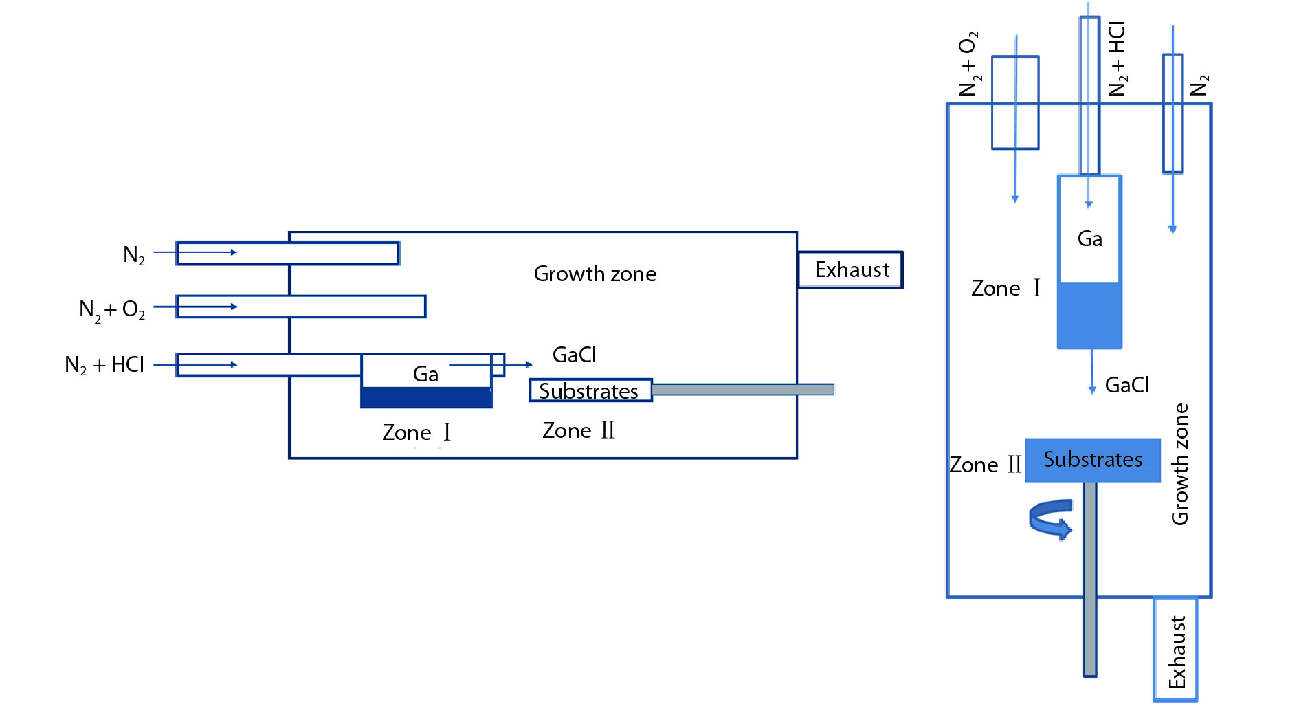
Gallium chloride has a variety of different valence states, e.g. GaCl, GaCl3, etc. GaCl is stable at high temperatures, and will decompose into GaCl3 below a certain temperature. This feature enables temperature adjustment of the reaction chamber to realize GaCl generation, transportation and deposition of Ga2O3. As a result, a typical HVPE growth system contains two reaction chambers at different temperatures, as shown in Fig. 1.
![]()
Figure 1.(Color online) Schematic diagram of (a) horizontal HVPE and (b) vertical HVPE.
As a cost-effective growth technique, HVPE supports production of high quality crystals with a faster growth rate. The fastest growth rate reported to date was ~250 μm/h for the growth of homoepitaxial layer on β-Ga2O3 (001) substrate[
To realize n-type doping of β-Ga2O3 thin films grown by HVPE, either SiCl4 or SnCl4 can be used as the efficient dopant source[
3. HVPE for the growth of polymorph Ga2O3
Note that the β-Ga2O3 structure is the most stable phase of Ga2O3, among the five different phases (α, β, γ, ε, and δ)[
3.1. β-Ga2O3 HVPE growth
The first HVPE growth of β-Ga2O3 has been reported by Matsumoto et al.[
![]()
Figure 2.(Color online) Optical photograph (unpublished) and SEM images of HVPE grown
3.2. α-Ga2O3 HVPE growth
α-Ga2O3 is also a very promising wide-bandgap semiconductor. α-Ga2O3 has been reported to have a large bandgap energy (Eg = 5.3 eV)[
Although trigonal corundum-structured α-Ga2O3 exists in a meta-stable phase compared to the β-Ga2O3 and cannot be obtained from the melt method, α-Ga2O3 has been hetero-epitaxially grown on sapphire substrates by HVPE[
α-Ga2O3 with the same corundum structure is the best lattice-matched polymorph with sapphire. The lattice mismatches between α-Ga2O3 and sapphire along the a- and c-axes are ~4.5 and ~3.3%, respectively. Although the lattice mismatch along the c-axis is considerably large, the pseudomorphic growth of α-Ga2O3 on α-Al2O3 can be stabilized because they share a common corundum structure. Once the first layer of α-Ga2O3 is formed, the structural similarity will promote the pseudomorphic growth.
It has been discovered that the deposition temperature was within the range of 525 to 650 °C[
3.3. ε-Ga2O3 HVPE growth
Epitaxial growths of the metastable ε-Ga2O3 phases have also been reported recently. Oshima[
Yao et al.[
![]()
Figure 3.(Color online) The cross-section HRTEM of
4. HVPE growth of Ga2O3 for nitride epitaxy and device application
Currently, HVPE growth of Ga2O3 focus on two areas. One is to grow the drift-layer for β-Ga2O3 Schottky barrier diodes, the other is to grow β-Ga2O3 films as the substrate or the buffer layers for III-nitrides epitaxy.
4.1. β-Ga2O3 Schottky barrier diodes
β-Ga2O3 is expected to have much larger Baliga’s figure of merit than SiC and GaN due to the predicted high breakdown electric field (~ 6–8 MV/cm) and high electron mobility (μ ~ 200–300 cm2/(V·s)). Currently, Schottky barrier diodes (SBDs) and FETs are being intensively investigated as the fundamental device components for power conversion systems. β-Ga2O3 based Schottky barrier diodes (SBDs) have been demonstrated, showing the reasonably good device characteristics[
In the early years, the development Ga2O3 SBDs was behind FETs, due mainly to a lack of suitable epitaxial growth techniques for the growth of thick n-Ga2O3 drift layer. In order to ensure the sufficient break down voltage, relatively thick n-Ga2O3 layers need to be grown with controlled thickness, good electrical conductivity in a cost-effective manner. HVPE method offers the possibility of growing this thick drift layer with high quality. Recently, the full-scale Ga2O3 SBDs were fabricated on epitaxial wafers with HVPE grown Si-doped n-Ga2O3 drift layers on n+-Ga2O3 (001) substrates[
![]()
Figure 4.(Color online) Schematic Ga2O3 SBD structure with an HVPE-grown n-Ga2O3 drift layer.
Until now, the highest reported breakdown voltage is ~1.1 kV for β-Ga2O3 drift-layer based field-plated SBD grown by HVPE[
![]()
Figure 5.(Color online) Schematic structure, forward and reverse
The above-mentioned results show that β-Ga2O3 Schottky rectifiers fabricated by HVPE technology are promising candidates for high power devices.
4.2. HVPE β-Ga2O3 films for III-nitrides epitaxy
β-Ga2O3 is also promising as substrate or buffer layer for epitaxial growth of GaN and related III-nitrides. Native GaN substrates are the best choice for the fabrication of III-nitride devices as only homoepitaxial growth provides the lowest defect density, zero lattice and thermal mismatch. However, native GaN substrates are costly and difficult to obtain despite recent progress in bulk GaN single crystal synthesis. For this reason, the majority of GaN-based devices are produced by heteroepitaxial growth on foreign substrates such as sapphire, Si or SiC. However, a lot of challenges still exist because of the insulating nature of sapphire, high price and high UV absorption of SiC, large lattice mismatch and chemical interaction of Si with GaN. As a result, bulk GaN remains prohibitive for the majority of device applications.
Sapphire is generally used as the substrate for GaN growth, but it is still limited because of poor lattice match (13.9%) and insulating nature of sapphire. In contrast, the lattice mismatch between β-Ga2O3 and GaN is significantly lower. β-Ga2O3 is excellent to serve as substrate for the growth of III-nitrides. It also combines the advantages of being transparent and conductive. Especially, high quality bulk β-Ga2O3 crystals can be produced by melt-growth techniques at low cost and high throughput.
As a result, there have been several reports published recently on the growth of GaN epilayers on differently oriented β-Ga2O3 substrates by MOVPE, MBE and HVPE[
Nikolaev et al.[
In these cases, high quality bulk crystal β-Ga2O3 have been used as the substrate for GaN epitaxy. However, bulk crystal β-Ga2O3 is still very expensive. Recently, we also have grown β-Ga2O3 thin films by HVPE[
5. Conclusions
In this paper, we have reviewed the HVPE growth and the latest progress in the area of the ultra-wide bandgap Ga2O3. It is concluded that HVPE is a promising candidate for the epitaxy of large-area Ga2O3 substrates and for the fabrication of Ga2O3-based high power devices. We also present discussions on the technological advantages and aspects of HVPE for epitaxy growth and high-power devices (such as SBDs) of Ga2O3. We expect that HVPE can be further developed as an all-purpose equipment for the large-scale, low-cost epitaxy of GaN and Ga2O3.
Acknowledgements
This work was supported by the National Key R&D Program of China (No. 2017YFB0404201), the Solid State Lighting and Energy-Saving Electronics Collaborative Innovation Center, PAPD, and the State Grid Shandong Electric Power Company.
References
[1] R Roy, V G Hill, E F Osborn et al. Polymorphism of Ga2O3 and the system Ga2O3–H2O. J Am Chem Soc, 74, 719(1952).
[2] H H Tippins. Optical absorption and photoconductivity in the band edge of
[3] H He, R Orlando, M A Blanco et al. First-principles study of structural, electronic, and optical properties of Ga2O3 in its monoclinic and hexagonal phases. Phys Rev B, 74, 195123(2006).
[4] M Orita, H Ohta, M Hirano et al. Deep-ultraviolet transparent conductive
[5] T Onuma, S Fujioka, T Yamaguchi et al. Correlation between blue luminescence intensity and resistivity in
[6] T Oshima, T Okuno, N Arai et al. Vertical solar-blind deep-ultraviolet Schottky photodetectors based on
[7] E G Víllora, K Shimamura, K Kitamura et al. Epitaxial relationship between wurtzite GaN and
[8] E G Víllora, S Arjoca, K Shimamura et al.
[9] K Sasaki, A Kuramata, T Masui et al. Device-quality
[10] M Higashiwaki, K Sasaki, A Kuramata et al. Gallium oxide (Ga2O3) metal–semiconductor field-effect transistors on single-crystal
[11] M Higashiwaki, K Sasaki, T Kamimura et al. Depletion-mode Ga2O3 metal–oxide–semiconductor field-effect transistors on
[12] Z Galazka, K Irmscher, R Uecker et al. On the bulk
[13] N Ueda, H Hosono, R Waseda et al. Anisotropy of electrical and optical properties in
[14] E G Villora, K Shimamura, Y Yoshikawa et al. Large-size
[15] A Kuramata, K Koshi, S Watanabe et al. High-quality
[16] T Oshima, T Okuno, S Fujita. Ga2O3 thin film growth on
[17] G Wagner, M Baldini, D Gogova et al. Homoepitaxial growth of
[18] K Fujito, S Kubo, H Nagaoka et al. Bulk GaN crystals grown by HVPE. J Cryst Growth, 311, 3011(2009).
[19] R Masuda, T Fujii, N Yoshii et al. Step-flow growth of homoepitaxial ZnO thin layers by halide vapor phase epitaxy using ZnCl2 and H2O source gases. J Cryst Growth, 312, 2324(2010).
[20] Y Kumagai, Y Kubota, T Nagashima et al. Preparation of a freestanding AlN substrate from a thick AlN layer grown by hydride vapor phase epitaxy on a bulk AlN substrate prepared by physical vapor transport. Appl Phys Express, 5, 055504(2012).
[21] K Nomura, K Goto, R Togashi et al. Thermodynamic study of
[22] Y Oshima, E G Vίllora, K Shimamura. Quasi-heteroepitaxial growth of
[23] N Suzuki, S Ohira, M Tanaka et al. Fabrication and characterization of transparent conductive Sn-doped
[24] M Slomski, N Blumenschein, P P Paskov et al. Anisotropic thermal conductivity of
[25] T Harwig, G J Wubs, G J Dirksen. Electrical properties of
[26] T Matsumoto, M Aoki, A Kinoshita et al. Absorption and reflection of vapor grown single crystal platelets of
[27] E G Víllora, K Shimamura, K Kitamura et al. Rf-plasma-assisted molecular-beam epitaxy of
[28] M Y Tsai, O Bierwagen, M E White et al.
[29] V Gottschalch, K Mergenthaler, G Wagner et al. Growth of
[30] W Mi, J Ma, Z Zhu et al. Epitaxial growth of Ga2O3 thin films on MgO (110) substrate by metal–organic chemical vapor deposition. J Cryst Growth, 354, 93(2012).
[31] F B Zhang, K Saito, T Tanaka et al. Structural and optical properties of Ga2O3 films on sapphire substrates by pulsed laser deposition. J Cryst Growth, 387, 96(2014).
[32] Z N Xiong, X Q Xiu, Y W Li et al. Growth of
[33] M Orita, H Hiramatsu, H Ohta et al. Preparation of highly conductive, deep ultraviolet transparent
[34] D Shinohara, S Fujita. Heteroepitaxy of corundum-structured
[35] T Kawaharamura, G T Dang, M Furuta. Successful growth of conductive highly crystalline Sn-doped
[36] K Akaiwa, S Fujita. Electrical conductive corundum-structured
[37] S Fujita, K Kaneko. Epitaxial growth of corundum-structured wide band gap III-oxide semiconductor thin films. J Cryst Growth, 401, 588(2014).
[38] Y Oshima, E G Víllora, K Shimamura. Halide vapor phase epitaxy of twin-free
[39] Y Oshima, E G Víllora, Y Matsushita et al. Epitaxial growth of phase-pure
[40] Y Yao, S Okur, A M Lyle et al. Growth and characterization of
[41] M Mohamed, K Irmscher, C Janowitz et al. Schottky barrier height of Au on the transparent semiconducting oxide
[42] S Oh, G Yang, J Kim. Electrical characteristics of vertical Ni/
[43] J Yang, S Ahn, F Ren et al. High reverse breakdown voltage Schottky rectifiers without edge termination on Ga2O3. Appl Phys Lett, 110, 192101(2017).
[44] M Higashiwaki, K Konishi, K Sasaki et al. Temperature-dependent capacitance–voltage and current–voltage characteristics of Pt/Ga2O3 (001) Schottky barrier diodes fabricated on n-Ga2O3 drift layers grown by halide vapor phase epitaxy. Appl Phys Lett, 108, 133503(2016).
[45] H Murakami, K Nomura, K Goto et al. Homoepitaxial growth of
[46] Z Z Hu, H Zhou, Q Feng et al. Field-plated lateral
[47] M Higashiwaki, K Sasaki, H Murakami et al. Recent progress in Ga2O3 power devices. Semicond Sci Technol, 31, 034001(2016).
[48] K Konishi, K Goto, H Murakami et al. 1-kV vertical Ga2O3 field-plated Schottky barrier diodes. Appl Phys Lett, 110, 103506(2017).
[49] K Shimamura, E G Víllora, K Domen et al. Epitaxial growth of GaN on (100)
[50] E G Víllora, K Shimamura, K Aoki et al. Molecular beam epitaxy of c-plane wurtzite GaN on nitridized a-plane
[51] Z L Xie, R Zhang, C T Xia et al. Demonstration of GaN/InGaN light emitting diodes on (100) beta-Ga2O3 substrates by metalorganic chemical vapour deposition. Chin Phys Lett, 25, 2185(2008).
[52] I A Ajia, Y Yamashita, K Lorenz et al. GaN/AlGaN multiple quantum wells grown on transparent and conductive (-201)-oriented
[53] V M Krymov, S I Stepanov, N K Zhumashev et al. GaN growth on
[54] S Ito, K Takeda, K Nagata et al. Growth of GaN and AlGaN on (100)
[55] H J Lee, T I Shin, D H Yoon. Influence of NH3 gas for GaN epilayer on
[56] K Kachel, M Korytov, D Gogova et al. A new approach to free-standing GaN using
[57] V I Nikolaev, A I Pechnikov, V N Maslov et al. GaN growth on
[58] Y W Li, X Q Xiu, Z N Xiong et al. Single crystal GaN layer converted from

Set citation alerts for the article
Please enter your email address
© Copyright 2018-2021 | Chinese Laser Press. All Rights Reserved 沪ICP备15018463号-20