• Journal of Semiconductors
  • Vol. 40, Issue 1, 011805 (2019)
Xiangqian Xiu, Liying Zhang, Yuewen Li, Zening Xiong, Rong Zhang, and Youdou Zheng
Author Affiliations
  • Key Laboratory of Advanced Photonic and Electronic Materials, School of Electronic Science and Engineering, Nanjing University, Nanjing 210023, China
  • show less
    DOI: 10.1088/1674-4926/40/1/011805 Cite this Article
    Xiangqian Xiu, Liying Zhang, Yuewen Li, Zening Xiong, Rong Zhang, Youdou Zheng. Application of halide vapor phase epitaxy for the growth of ultra-wide band gap Ga2O3[J]. Journal of Semiconductors, 2019, 40(1): 011805 Copy Citation Text show less

    Abstract

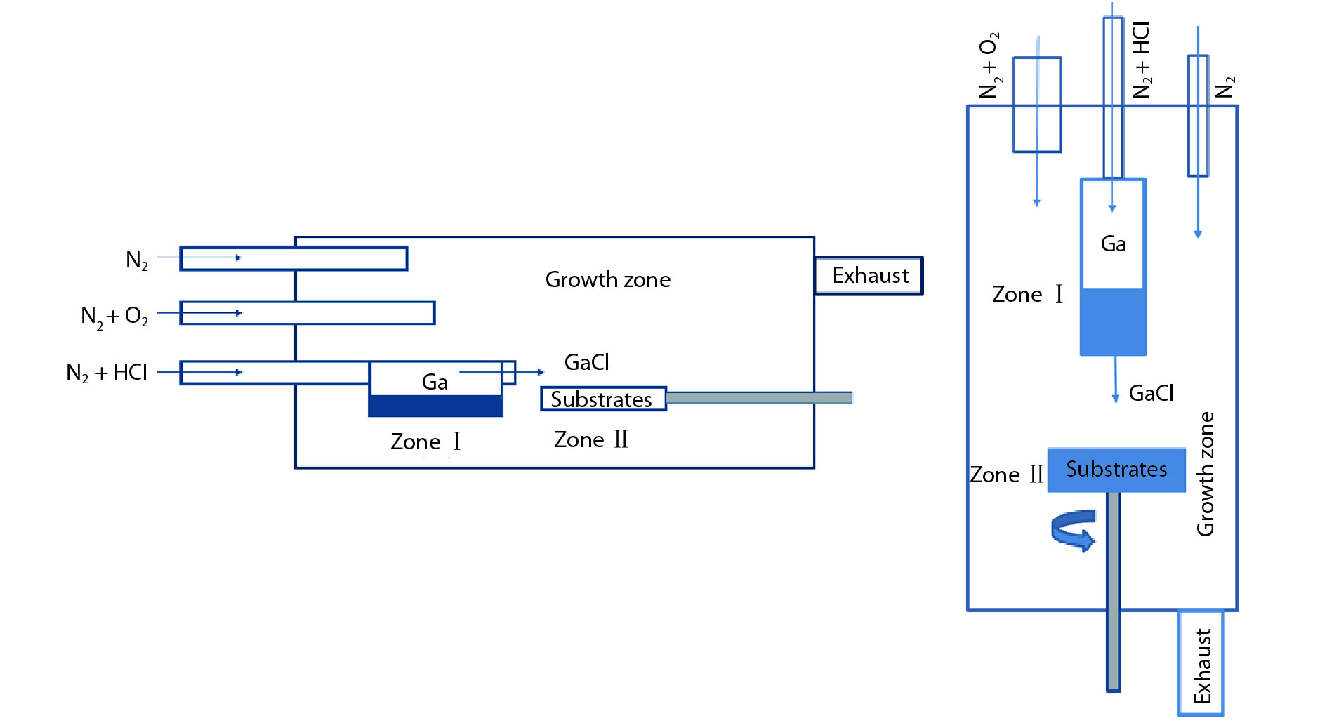
    Halide vapor phase epitaxy (HVPE) is widely used in the semiconductor industry for the growth of Si, GaAs, GaN, etc. HVPE is a non-organic chemical vapor deposition (CVD) technique, characterized by high quality growth of epitaxial layers with fast growth rate, which is versatile for the fabrication of both substrates and devices with wide applications. In this paper, we review the usage of HVPE for the growth and device applications of Ga2O3, with detailed discussions on a variety of technological aspects of HVPE. It is concluded that HVPE is a promising candidate for the epitaxy of large-area Ga2O3 substrates and for the fabrication of high power β-Ga2O3 devices.
    ${\rm{Ga}}\left( {\rm{s}} \right) + {\rm{HCl}}\left( {\rm{g}} \right) \to {\rm{GaCl}}\left( {\rm{g}} \right) + {{\rm H}_2}\left( {\rm g} \right),$ ()

    View in Article

    ${\rm{GaCl}}\left( {\rm{g}} \right) + {\rm O_2}\left( {\rm g} \right) \to {\rm G{a_2}{O_3}}\left( {\rm s} \right) + {\rm C{l_2}}\left( {\rm g} \right).$ ()

    View in Article

    Xiangqian Xiu, Liying Zhang, Yuewen Li, Zening Xiong, Rong Zhang, Youdou Zheng. Application of halide vapor phase epitaxy for the growth of ultra-wide band gap Ga2O3[J]. Journal of Semiconductors, 2019, 40(1): 011805
    Download Citation