
Tianlun Shen, Jinhai Si, Tao Chen, Xun Hou. Application of Femtosecond Laser Irradiation and Wet Etching in Fabrication of Microstructures in Crystal Materials[J]. Laser & Optoelectronics Progress, 2020, 57(11): 111419
- Laser & Optoelectronics Progress
- Vol. 57, Issue 11, 111419 (2020)
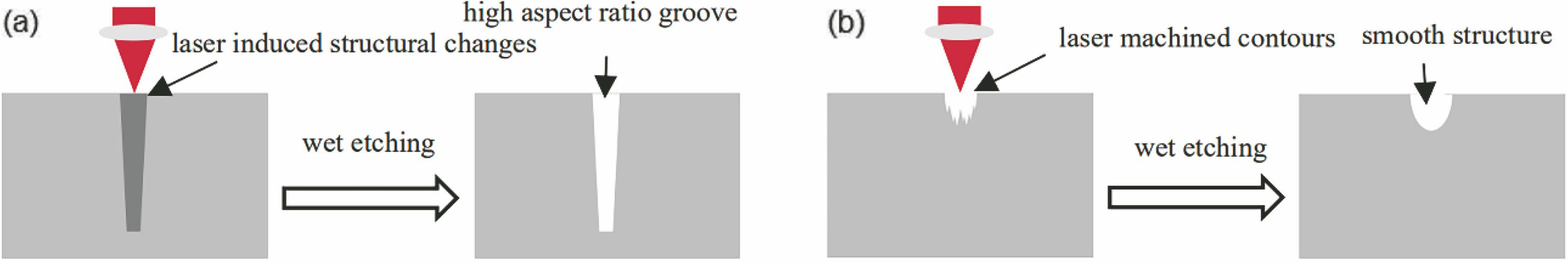
Fig. 1. Flow chart of femtosecond laser irradiation and wet etching. (a) Fabrication of high aspect ratio groove by femtosecond laser irradiation and wet etching; (b) fabrication of micro-lens by femtosecond laser irradiation and wet etching
![Schematic of sapphire transition from crystal structure to amorphous structure under femtosecond laser[36]](/richHtml/lop/2020/57/11/111419/img_2.jpg)
Fig. 2. Schematic of sapphire transition from crystal structure to amorphous structure under femtosecond laser[36]
Fig. 3. Morphology of structure changes and the chemical selective etching induced grooves[44]. (a)(b) Optical micro-scope images of structure change regions before and after chemical etching induced by lens focused femtosecond laser; (c) SEM image of Fig. 3 (b); (d)(e) optical micro-scope images of structure change regions before and after chemical etching induced by micro-scope objective lens focused femtosecond lase
Fig. 4. SEM images of honeycomb arrays of micro-holes fabricated by femtosecond laser irradiation and selective chemical etching[21]. (a) Hole entrances for the sample fabricated at laser power of 30 mW and pulse number of 4000; (b) hole entrances for the sample fabricated at laser power of 45 mW and pulse number of 1600
Fig. 5. SEM images of various structures[45]. (a) Chinese dragon; (b) line array; (c) circular ring; (d) rings array; (e) triangular; (f) square; (g) pentagon
Fig. 6. SEM images of various designed suspended structures[45]. (a) Suspended line; (b) suspended disk; (c) suspended helix; (d) suspended hexagon
Fig. 7. Convex grid-patterned microstructures induced by wet etching assisted femtosecond laser[47]. (a) SEM image of Si sample after femtosecond laser irradiation; (b)(c) perpendicular and sloping images of the obtained convex microstructures; (d) morphology of the microstructures achieved by LCM; (e) height of the microstructures in different position
Fig. 8. Process of imaging MLA with a fill factor of 96.6%[26]. (a) Imaging device; (b) image array
Fig. 9. Experimental results by parallel fabrication of femtosecond laser irradiation assisted wet etching. (a) Groove with high aspect ratio[49]; (b) micro-lens array[50]
Fig. 10. Silicon carbide processed by femtosecond laser irradiation and wet etching. (a) Groove with high aspect ratio[22]; (b) through hole structure[23]
Fig. 11. SEM images of micro-channel morphology of silicon carbide. (a) SEM image after laser irradiation; (b) magnified view of the laser irradiation modified area marked with rectangle 1 in Fig. 1 (a); (c) micro-channel after treatment with HF; (d) magnified view of the micro-channel[54]
Fig. 12. Grating structure processed by femtosecond laser irradiation and wet etching[55]. (a) SiC grating structure(100×); (b) diffraction pattern of SiC grating structure captured by camera
Fig. 13. Morphology and chemical composition of silicon carbide grating structure before and after chemical corrosion[59]. (a) Morphology before corrosion; (b) chemical composition in zone A; (c) morphology after corrosion; (d) chemical composition in zone B
Fig. 14. Influence of polarization on nano-ripples[27]. (a) E perpendicular to the hole-wall surface; (b) the angle of E and the hole-wall surface is 45°; (c) E is parallel to the hole-wall surface
Fig. 15. Sapphire processed by femtosecond laser. (a) 3D channel structure[37]; (b) deep hole structure[40]; (c) nanopore structure[60]
Fig. 16. Sapphire micro-optical devices prepared by femtosecond laser irradiation and wet etching. (a) AFM characterization exhibiting 3D morphology and the cross section at the central line of the FZP[62]; (b) SEM images and the diffraction efficiency of the Dammann gratings that generate 5×5 spot sources[63]; (c) SEM image of SWSs on sapphire after etching and measured transmittance of fabricated SWSs on
Fig. 17. Imaging performance of the concave micro-lens array[65]. (a) Schematic illustration of the imaging system; (b) optical images of the concave micro-lens array on a paper printed with JLU, the square region is the concave micro-lens array; (c)(d) image array of letter “F” using the concave micro-lens arrays with spacing of 25 μm and 40 μm, and the corresponding scale bars are 50 μm and 80 μm, respectively

Set citation alerts for the article
Please enter your email address
© Copyright 2018-2021 | Chinese Laser Press. All Rights Reserved 沪ICP备15018463号-20