• Photonics Research
  • Vol. 12, Issue 1, 115 (2024)
Jianing Wang1、2, Xi Wang1、2, Yihang Li1、2, Yanfu Yang2, Qinghai Song1、3, and Ke Xu1、2、*
Author Affiliations
  • 1Guangdong Provincial Key Laboratory of Semiconductor Optoelectronic Materials and Intelligent Photonic Systems, Harbin Institute of Technology, Shenzhen 518055, China
  • 2Department of Electronic & Information Engineering, Harbin Institute of Technology, Shenzhen 518055, China
  • 3Department of Science, Harbin Institute of Technology, Shenzhen 518055, China
  • show less
    DOI: 10.1364/PRJ.508024 Cite this Article Set citation alerts
    Jianing Wang, Xi Wang, Yihang Li, Yanfu Yang, Qinghai Song, Ke Xu. High-responsivity on-chip waveguide coupled germanium photodetector for 2 μm waveband[J]. Photonics Research, 2024, 12(1): 115 Copy Citation Text show less
    (a) Three-dimensional schematic diagram of the SACM APD. (b) Cross-section schematic diagram of the SACM APD. Standard silicon-on-insulator (SOI) with 220 nm top silicon and 2 μm buried oxide used as substrates. The 300 nm wide P doping is designed as a charge region, and the intrinsic silicon is designed as a multiplication region with width of Wi. The heavily doped N++ and P++ regions located in both sides of the silicon slab serve as connection regions. These regions are connected to the Al electrode through tungsten (W) vias. A 600 nm×260 nm germanium acts as absorption region. Inset, simulated electric field profile of the fundamental TE-polarized optical mode at 1950 nm wavelength at the Ge layer.
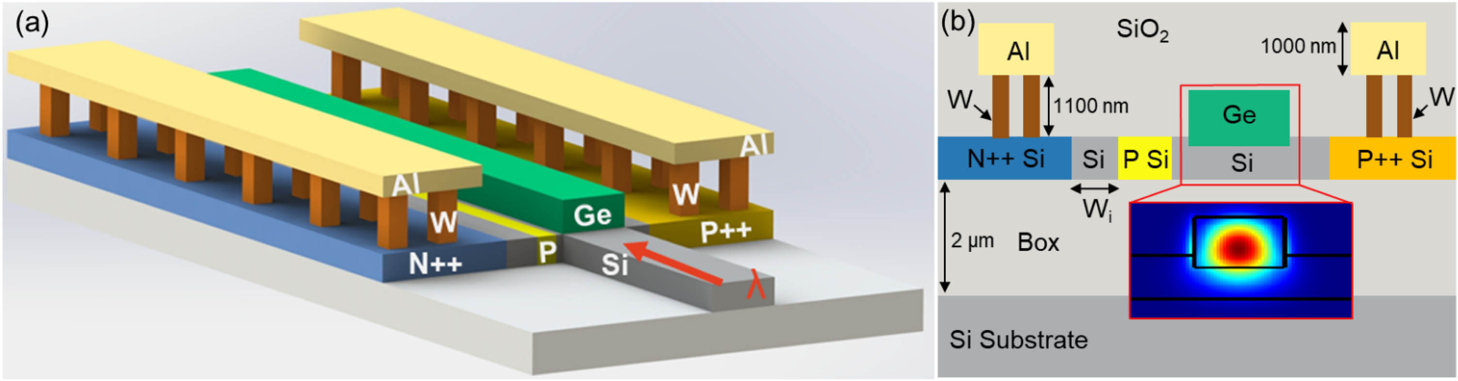
    Fig. 1. (a) Three-dimensional schematic diagram of the SACM APD. (b) Cross-section schematic diagram of the SACM APD. Standard silicon-on-insulator (SOI) with 220 nm top silicon and 2 μm buried oxide used as substrates. The 300 nm wide P doping is designed as a charge region, and the intrinsic silicon is designed as a multiplication region with width of Wi. The heavily doped N++ and P++ regions located in both sides of the silicon slab serve as connection regions. These regions are connected to the Al electrode through tungsten (W) vias. A 600  nm×260  nm germanium acts as absorption region. Inset, simulated electric field profile of the fundamental TE-polarized optical mode at 1950 nm wavelength at the Ge layer.
    (a) Simulated electric field distribution at the central vertical cross section of device A with −29 V bias. (b) Simulated electric field distribution at the central vertical cross section of device B with −22 V bias. (c) Electric field distribution along the cutline of (a) and (b).
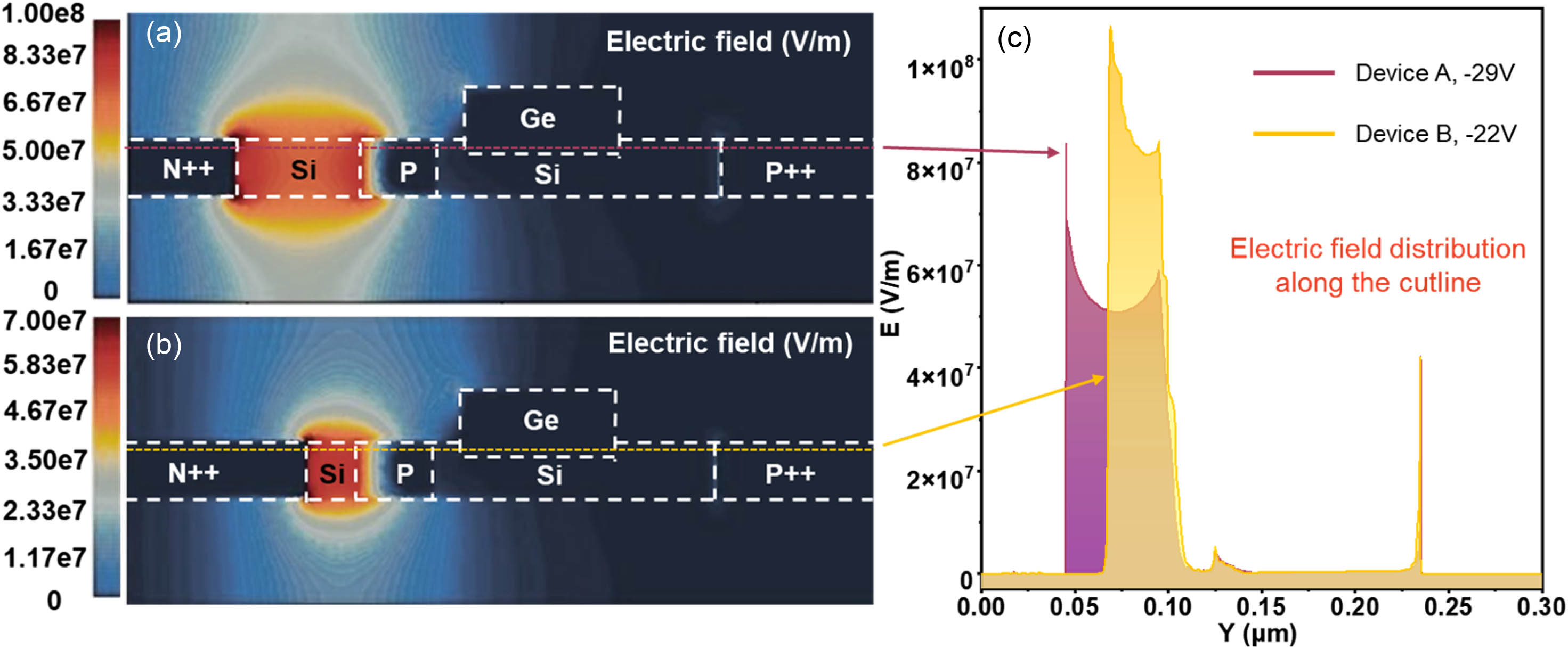
    Fig. 2. (a) Simulated electric field distribution at the central vertical cross section of device A with 29  V bias. (b) Simulated electric field distribution at the central vertical cross section of device B with 22  V bias. (c) Electric field distribution along the cutline of (a) and (b).
    Static measurements of designed SACM APD at 1950 nm with 0 dBm input power. The blue line represents the measured results of the device A, and the red line represents the measured results of device B. (a) Measured I-V characteristics. The dashed line represents the dark current, and the solid line represents the illuminated current. (b) Measured responsivity as a function of bias voltage. (c) Measured gain as a function of bias voltage. (d) Measured responsivity of the SACM APD versus input wavelength from 1480–1640 nm to 1950–2045 nm. The bias voltages of devices A and B are −29 V and −22 V, respectively. At a wavelength range of 1480–1640 nm, the input power is −18 dBm; at 1950–2045 nm, the input power is 0 dBm.
    Fig. 3. Static measurements of designed SACM APD at 1950 nm with 0 dBm input power. The blue line represents the measured results of the device A, and the red line represents the measured results of device B. (a) Measured I-V characteristics. The dashed line represents the dark current, and the solid line represents the illuminated current. (b) Measured responsivity as a function of bias voltage. (c) Measured gain as a function of bias voltage. (d) Measured responsivity of the SACM APD versus input wavelength from 1480–1640 nm to 1950–2045 nm. The bias voltages of devices A and B are 29  V and 22  V, respectively. At a wavelength range of 1480–1640 nm, the input power is 18  dBm; at 1950–2045 nm, the input power is 0 dBm.
    Experimental setup of measuring bandwidth and eye diagrams. The solid blue line represents the optical connection, while the dotted dark line represents the electrical connection. Inset, top-view microscope image of the fabricated device.
    Fig. 4. Experimental setup of measuring bandwidth and eye diagrams. The solid blue line represents the optical connection, while the dotted dark line represents the electrical connection. Inset, top-view microscope image of the fabricated device.
    (a) Equivalent circuit for cross section view of the SACM APD. (b) Equivalent circuit for top view of the SACM APD. (c) Equivalent circuit of the SACM APD. The blue area represents the SACM APD waveguide region, yellow represents the electrode section, and orange represents the load part.
    Fig. 5. (a) Equivalent circuit for cross section view of the SACM APD. (b) Equivalent circuit for top view of the SACM APD. (c) Equivalent circuit of the SACM APD. The blue area represents the SACM APD waveguide region, yellow represents the electrode section, and orange represents the load part.
    Simulated normalized S21 response versus frequency under different bias voltages for devices (a) A and (b) B.
    Fig. 6. Simulated normalized S21 response versus frequency under different bias voltages for devices (a) A and (b) B.
    (a) Measured normalized frequency response for both devices. The blue line represents the measured frequency response of device A at −29 V bias, and the red line represents the measured frequency response of device B at −22 V bias. Measured NRZ-OOK eye diagram of device A at bit rates of (b) 12 Gbit/s and (c) 16 Gbit/s. Measured NRZ-OOK eye diagram of device B at bit rates of (d) 16 Gbit/s and (e) 20 Gbit/s.
    Fig. 7. (a) Measured normalized frequency response for both devices. The blue line represents the measured frequency response of device A at 29  V bias, and the red line represents the measured frequency response of device B at 22  V bias. Measured NRZ-OOK eye diagram of device A at bit rates of (b) 12 Gbit/s and (c) 16 Gbit/s. Measured NRZ-OOK eye diagram of device B at bit rates of (d) 16 Gbit/s and (e) 20 Gbit/s.
    3 dB bandwidth and GBP versus avalanche multiplication gain for devices (a) A and (b) B.
    Fig. 8. 3 dB bandwidth and GBP versus avalanche multiplication gain for devices (a) A and (b) B.
    Cj (fF)Cload (Ω)Rs (Ω)Re (Ω)Rload (Ω)Le (pH)
    Device A (29  V)81.32166.0186.271.1850167.5
    Device B (22  V)106.19169.598.001.2450163.5
    Table 1. Calculated Parasitic Parameter Used in the Equivalent Circuit
    ReferencesMaterialλ (μm)Responsivity (A/W)Bandwidth (GHz)Bit Rate (Gbit/s)
    [28]Defect-mediated Si2.020.3 at 30  V12.5 at 30  V28 at 27  V
    [29]Defect-mediated Si1.90.35 at 25  V1 at 25  V
    [30]Ge1.970.08 at 21.4  V
    This work (device A)Ge1.951.05 at29  V6.12 at29  V16 at29  V
    This work (device B)Ge1.950.71 at22  V7.12 at22  V20 at22  V
    Table 2. Summary of the Reported 2 μm Band PDs Made by the Silicon Photonics Platform
    Jianing Wang, Xi Wang, Yihang Li, Yanfu Yang, Qinghai Song, Ke Xu. High-responsivity on-chip waveguide coupled germanium photodetector for 2 μm waveband[J]. Photonics Research, 2024, 12(1): 115
    Download Citation