1Guangdong Provincial Key Laboratory of Semiconductor Optoelectronic Materials and Intelligent Photonic Systems, Harbin Institute of Technology, Shenzhen 518055, China
2Department of Electronic & Information Engineering, Harbin Institute of Technology, Shenzhen 518055, China
3Department of Science, Harbin Institute of Technology, Shenzhen 518055, China
【AIGC One Sentence Reading】:We developed a high-performance on-chip germanium photodetector for the 2 μm waveband, featuring high responsivity and speed, overcoming challenges in silicon photonic integrated circuits for this emerging waveband.
【AIGC Short Abstract】:In this study, we presented a high-performance on-chip waveguide-coupled germanium photodetector tailored for the 2 μm waveband. Through a novel absorption charge multiplication structure, the detector achieved enhanced sub-bandgap absorption, boasting a responsivity of 1.05 A/W and a 3 dB bandwidth of 7.12 GHz, capable of receiving high-speed signals at up to 20 Gbit/s. This innovation bridges the gap between silicon photonic circuits and emerging 2 μm waveband applications.
Note: This section is automatically generated by AI . The website and platform operators shall not be liable for any commercial or legal consequences arising from your use of AI generated content on this website. Please be aware of this.
Abstract
Recently, the emerging 2 μm waveband has gained increasing interest due to its great potential for a wide scope of applications. Compared with the existing optical communication windows at shorter wavelengths, it also offers distinct advantages of lower nonlinear absorption, better fabrication tolerance, and larger free carrier plasma effects for silicon photonics, which has been a proven device technology. While much progress has been witnessed for silicon photonics at the 2 μm waveband, the primary challenge still exists for on-chip detectors. Despite the maturity and compatibility of the waveguide coupled photodetectors made of germanium, the 2 μm regime is far beyond its cutoff wavelength. In this work, we demonstrate an efficient and high-speed on-chip waveguide-coupled germanium photodetector operating at the 2 μm waveband. The weak sub-bandgap absorption of epitaxial germanium is greatly enhanced by a lateral separation absorption charge multiplication structure. The detector is fabricated by the standard process offered by a commercial foundry. The device has a benchmark performance with responsivity of 1.05 A/W and 3 dB bandwidth of 7.12 GHz, which is able to receive high-speed signals with up to 20 Gbit/s data rate. The availability of such an efficient and fast on-chip detector circumvents the barriers between silicon photonic integrated circuits and the potential applications at the 2 μm waveband.
1. INTRODUCTION
Exploiting larger bandwidth and higher data capacity is a long-standing pursuit for a huge community of optical communications. The existing C + L band may not be able to provide enough data channels to meet this demand from a long-term point of view. An alternative and promising spectral region near 2 μm has attracted increasing interests. It offers low-attenuation in hollow-core photonic bandgap fibers [1] and broad gain bandwidth in thulium-doped fibers [2]. It also has great potential for free-space optical communications due to its eye-safety [3] and atmospheric transparency [4]. Due to the less mature device technologies in this particular waveband, several preliminary experiments of optical transmissions in fiber and free space have been demonstrated using discrete packaged components [4–8]. Driven by these prospects, an increasing amount of research effort has been directed to developing integrated silicon photonics at 2 μm. A variety of components have been reported in recent years including grating couplers [9], arrayed waveguide gratings (AWGs) [10], power splitters [11,12], modulators [13–16], filters [17,18], and switches [19].
However, on-chip photodetection remains challenging for silicon photonics at 2 μm band due to the transparency of germanium. One possible way to overcome this challenge is to integrate heterogeneous materials with suitable bandgaps on silicon. For example, III-V materials such as InGaAs [20,21] and InGaAsSb [22] can be bonded on the silicon-on-insulator (SOI) substrate via mature techniques. Another way is heterogeneous integration of the absorbing material of GeSn. Its bandgap can be flexibly controlled by adjusting the element composition. It gives rise to several demonstrations of efficient GeSn photodetectors on silicon substrate at longer wavelengths [23–25]. The great variety of 2D materials with different bandgaps are also alternative candidates for photodetectors beyond the cutoff wavelengths of conventional bulk materials. While graphene and black phosphorus have been integrated on silicon waveguides via van der Waals forces for on-chip detectors at 2 μm wavelengths [26], it is hardly compatible with the standard silicon photonic fabrication process. Similar issues are associated with the HgTe quantum dot detectors [27]. Besides intrinsic absorption, a silicon photodetector has been demonstrated by enhanced defect state absorption [28,29]. Though intermediate absorption can be achieved without introducing additional materials, it requires additional ion implantation processing.
Since a weak absorption can be observed in epitaxial germanium due to the indirect band absorption [30], here we demonstrate a germanium photodetector with significantly enhanced responsivity by a simple separation absorption charge multiplication (SACM) structure [31].
Sign up for Photonics Research TOC. Get the latest issue of Photonics Research delivered right to you!Sign up now
Different from the previous study where additional silicon deposition is required, the proposed SACM avalanche photodetector (APD) incorporates the multiplication layer in a lateral structure, which simplifies the fabrication process. This design leads to higher responsivity, lower noise, and better CMOS compatibility [32].
2. DESIGN AND FABRICATION
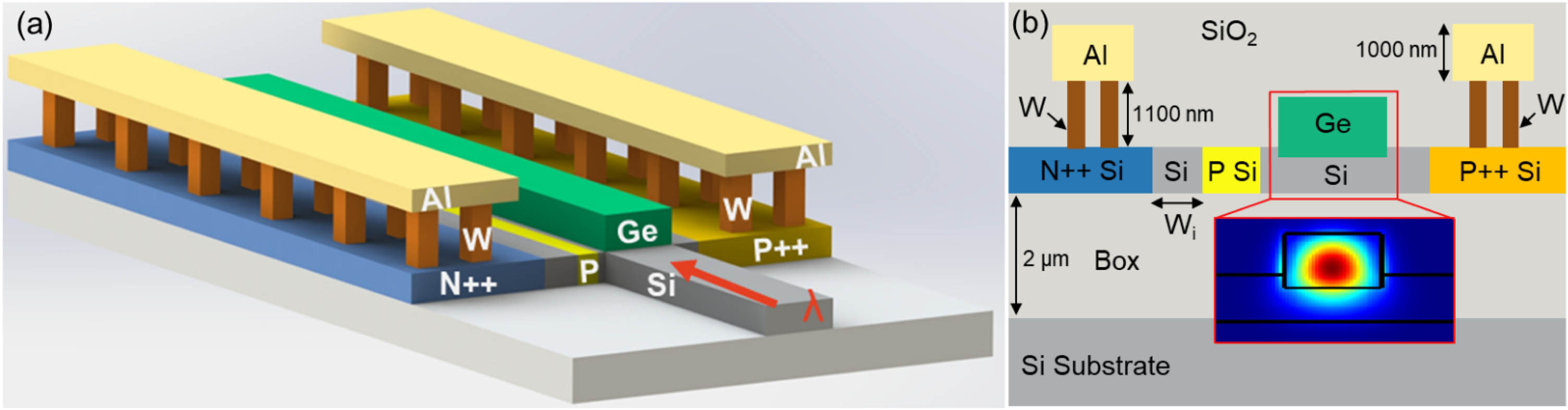
The proposed SACM APD is designed on standard SOI with 220 nm top silicon and 2 μm buried oxide. The three-dimensional schematic diagram of the SACM APD is shown in Fig. 1(a). The incident optical wave is incident into the absorption layer through the silicon waveguide and then evanescently coupled to the germanium absorption layer on top of the silicon. As shown by the cross-section view in Fig. 1(b), the heavily doped regions of P++ and N++ are formed by ion implantation of boron and phosphorus with concentration of and , respectively. The P++ and N++ regions have low resistance and are used for connection with the Al metal layer through vertical contact vias with 1100 nm height. The 1000 nm thick Al metal layer is used as an electrical interconnection layer. Between the N++ regions and the silicon waveguide, a 300 nm wide P charge layer doped with boron and an intrinsic multiplication layer with width of are designed. Here, P-type doping is selected as the charge layer since electrons have a significantly higher ionization coefficient than holes [33]. The separated charge layer greatly enhances the electric field across the multiplication layer where the avalanche effect takes place. On top of the silicon waveguide, a 260 nm thick epitaxy Ge absorption layer is deposited with dimensions of μμ. The inset diagram in Fig. 1(b) illustrates the simulated TE mode electric field at a wavelength of 1950 nm. It can be seen that the majority of the mode is confined within the Ge absorption layer. To investigate the performance trade-off between the responsivity and electrical bandwidth, two types of photodetectors with different multiplication layer widths () of 500 nm (device A) and 200 nm (device B) are designed for comparison. The length of the active region is chosen to be 800 μm to ensure complete absorption. The electrode pad dimensions are μμ with a spacing of 150 μm. Two electrodes are configured for such an SACM APD structure with lateral junction.
Figure 1.(a) Three-dimensional schematic diagram of the SACM APD. (b) Cross-section schematic diagram of the SACM APD. Standard silicon-on-insulator (SOI) with 220 nm top silicon and 2 μm buried oxide used as substrates. The 300 nm wide P doping is designed as a charge region, and the intrinsic silicon is designed as a multiplication region with width of . The heavily doped N++ and P++ regions located in both sides of the silicon slab serve as connection regions. These regions are connected to the Al electrode through tungsten () vias. A germanium acts as absorption region. Inset, simulated electric field profile of the fundamental TE-polarized optical mode at 1950 nm wavelength at the Ge layer.
The device is fabricated by a standard silicon photonic process via the multi-project wafer (MPW) shuttle run offered by a commercial foundry. The waveguide is first defined by photolithography followed by a single-step dry etching. The germanium layer is grown on silicon through an epitaxial process. Following this process, cyclic thermal annealing is required. Due to the mismatch in the thermal expansion coefficients of germanium and silicon [34], annealing will induce a weak tensile strain on germanium, resulting in a shrinkage in the bandgap. The doping regions are realized by ion implantations with different dosages. Contact vias are fabricated by etching through the cladding dielectric layer. Then, a pair of electrodes are formed by metal deposition. It is noted that the SOI substrate and the fabrication process are all the same for manufacturing silicon photonic components at the conventional C-band.
3. RESULTS
To verify the field enhancement of the SACM structure, the finite element method (FEM) is used to simulate the electric field distribution across the APD. The field distributions under bias on device A and on device B are shown in Figs. 2(a) and 2(b), respectively. The estimated electric field intensity in the multiplication region is as high as for device A and for device B. Such a high field intensity allows for acceleration of the photo-generated electrons, which is followed by the avalanche effect. This will significantly enhance the responsivity of the germanium PD, which has weak sub-bandgap absorption at the 2 μm waveband. It also ensures that the carriers drift at saturation velocity; hence, the electrical bandwidth is only constrained by the RC constant of the device.
Figure 2.(a) Simulated electric field distribution at the central vertical cross section of device A with bias. (b) Simulated electric field distribution at the central vertical cross section of device B with bias. (c) Electric field distribution along the cutline of (a) and (b).
It should be noted that the sub-bandgap absorption mainly comes from two aspects. First, it is difficult to completely eliminate the defect via annealing process [35]. These defects serve as recombination centers [34], causing the absorption wavelength to shift toward longer wavelengths [36]. Second, the thermal annealing process induces dopant diffusion into the intrinsic region [37], and it will introduce impurity levels into the forbidden band. Both effects contribute to the absorption at the extended waveband beyond the band edge of germanium [38].
The electric field distributions of both devices A and B are numerically simulated and plotted in Fig. 2(c). The electric field intensity in the Ge absorption region is kept below for both cases, which can effectively prevent excessive noise caused by Ge ionization [39]. The narrow intensity peaks of the electric field appearing in the interfaces of different doping regions are mainly caused by the built-in electric field formed by the diffusion of the majority carriers. To characterize the SACM APD, a high-precision source meter (Keithley 2450) is first used to measure the static I-V curve. The input incident optical power is estimated by normalizing the coupling loss of the edge coupler, which is 4.3 dB/facet. The transition loss from silicon to the germanium layer can be considered to be negligible. The I-V curves for both devices A and B are measured under dark condition and 0 dBm input power of 1950 nm, as indicated by dotted and solid lines in Fig. 3(a). When the reverse bias voltages are lower than for device A and for device B, the dark currents of both APDs are measured at a low level below 10 nA. Device B has a slightly larger dark current than device A due to the higher field intensity. Under 0 dBm illumination, the photocurrents of devices A and B reach 1.05 mA and 0.71 mA under the bias of and , respectively. The breakdown voltages of both devices are estimated to be 27.2 V and 16.6 V, respectively. It should be noted that such high responsivity can only be achieved under the avalanche mode with large-enough bias. Figure 3(b) shows the responsivity as a function of different reverse bias voltages measured at a wavelength of 1950 nm. A responsivity as high as 1.05 A/W is measured at bias for device A and 0.71 A/W at bias for device B. It is important to note that the incident power used for responsivity estimation is normalized with the fiber-chip coupling loss only. In fact, the waveguide transition and evanescent coupling might induce additional losses that have not been considered. Hence, the responsivity might be slightly underestimated here. According to the literature review, the responsivity of the proposed device represents the state-of-the-art performance of the on-chip photodetectors operating at the 2 μm waveband. It is also comparable with the commercial product made of InGaAs. To quantify the avalanche effect, we calculate the multiplication gain of the SACM APD, as shown in Fig. 4(c). First, the unit-gain region is defined at the flat part of the I-V plot [40–42]. Here, the unit-gain voltage is estimated to be for device A and for device B, respectively. The avalanche multiplication gain can then be calculated by the ratio of the responsivity at bias voltage to the responsivity at unit-gain voltage. It can be seen from Fig. 4(c) that the multiplication gain increases exponentially above the unit-gain voltages. When the measured photocurrent reaches the order of mA, a maximum gain of 91.3 can be achieved for device A. Since device B has a thinner multiplication layer that renders the device with stronger avalanche effect, a much higher gain of 151.3 can be achieved. The high gain allows for significant enhancement in responsivity of the germanium APD operated at 2 μm wavelengths.
Figure 3.Static measurements of designed SACM APD at 1950 nm with 0 dBm input power. The blue line represents the measured results of the device A, and the red line represents the measured results of device B. (a) Measured I-V characteristics. The dashed line represents the dark current, and the solid line represents the illuminated current. (b) Measured responsivity as a function of bias voltage. (c) Measured gain as a function of bias voltage. (d) Measured responsivity of the SACM APD versus input wavelength from 1480–1640 nm to 1950–2045 nm. The bias voltages of devices A and B are and , respectively. At a wavelength range of 1480–1640 nm, the input power is ; at 1950–2045 nm, the input power is 0 dBm.
Figure 4.Experimental setup of measuring bandwidth and eye diagrams. The solid blue line represents the optical connection, while the dotted dark line represents the electrical connection. Inset, top-view microscope image of the fabricated device.
To study the characteristic of SACM APD’s broad band response, we measure the responsivity from the S-band to the extended 2 μm waveband. Constrained to the availability of the broadband tunable laser, the measurement covers spectral range of the S-band, C-band, L-band, U-band, and 2 μm waveband. Since germanium has much more efficient absorption at short wavelengths, the incident power in the 1480–1640 nm range is set to be to avoid saturation. It is chosen to be 0 dBm for the 1950–2045 nm range, which is limited by the laser output spectral range. The testing results for different wavebands are obtained and plotted in Fig. 3(d). The results have been normalized by factoring out the coupling loss spectra of the edge coupler. Within the wavelength range of 1480 nm to 1530 nm, despite the less efficient absorption of germanium at longer wavelengths [34], the responsivity has a slight increase with the wavelengths. In contrast, the responsivity gradually decreases toward long wavelength within the range of 1530 nm to 1580 nm, which is due to the less efficient absorption of germanium. Within the range of 1580 nm to 1640 nm, the responsivity curve tends to be flat. Beyond that, the response can be expected to be significantly weaker even though we are not able to measure the device beyond wavelength of 1640 nm. The peak responsivity is measured to be 7.04 A/W at 1530 nm. Starting from 1950 nm to 2050 nm, the responsivity can be measured by using another laser operated for the 2 μm waveband. As described before, the responsivity drops to 1.05 A/W at 1950 nm. Though we are not able to measure the wavelength range in between, it is reasonable to expect that the APD can operate across the whole spectral range of measurement with responsivity of the order of A/W. These results suggest that the proposed SACM APDs can be potentially applied to broadband optical communication systems from the S-band to the 2 μm band.
In order to characterize the high-speed photodetection performance at the 2 μm waveband, electrical bandwidth and eye diagram measurements are performed. The experimental setup for measuring the bandwidth and eye diagram is shown in Fig. 4. A continuous wave (CW) is emitted by a narrow linewidth laser and then passes through a home-made three-paddle polarization controller (PC) using SM-1950 jump fiber. The CW is then modulated by a commercial high-speed lithium niobate modulator with a bandwidth of 35 GHz. The signal is fed into the silicon chip via an edge coupler. A high-frequency bias tee with 40 GHz bandwidth is used to couple the DC and AC signals between the SACM APD and measurement instruments. The source meter (2450 Keithley, USA) is used to supply bias voltage and measure the photocurrent with pA precision. It also allows for setting a current limit to prevent breakdown. The vector network analyzer (VNA, E5063A, Keysight, USA) is applied to measure the small-signal frequency response for electrical bandwidth analysis. The cable and bias tee have been calibrated using the calibration kit. The pseudo-random binary sequence (PRBS) of a non-return-to-zero (NRZ) pattern with length of is generated by a pulse pattern generator (PPG, SL3120A, Sionlink, China). The baseband signal is then amplified by an RF wide band amplifier. A high-speed sampling oscilloscope (DSA8300, Tektronix, USA) is synchronized by an external clock generated by the PPG. The eye diagram of the high-speed signals can be captured and analyzed by the oscilloscope.
Here, the comprehensive bandwidth analysis of the SACM APD is performed. As mentioned above, the carriers are able to drift at saturation velocity under the bias condition for avalanche effect. Hence, the electrical bandwidth is mainly constrained by the RC constant of the device. The bandwidth of the device is evaluated based on the equivalent circuit model of the devices. Figure 5(a) shows the cross-section view of the proposed SACM APD and its corresponding equivalent circuit. The current source represents the generated current after the carrier multiplication process. The parameter represents the junction capacitance resulting from the built-in electric field in the multiplication region. Another symbol represents the slab series resistance. Figure 5(b) shows the top-view of the SACM APD, which describes the electrode arrangement and the corresponding equivalent circuit.
Figure 5.(a) Equivalent circuit for cross section view of the SACM APD. (b) Equivalent circuit for top view of the SACM APD. (c) Equivalent circuit of the SACM APD. The blue area represents the SACM APD waveguide region, yellow represents the electrode section, and orange represents the load part.
The electrode parasitic parameters include the parasitic resistance , inductance , and capacitance between PAD and electrode, as well as the external load . By combining the circuits of cross-section view and top-view, the overall equivalent circuit of the SACM APD can be obtained as is shown in Fig. 5(c). By performing Laplace transform and Thevenin equivalence on the circuit, the transfer function is given by where and are given by
The parasitic parameters depicted in Fig. 5(c) are numerically solved from simulations via the finite element method. The obtained results are summarized in Table 1. Then, the 3 dB bandwidth can be obtained by solving the equation . To further estimate the bandwidth, we numerically calculated the response using the transmission matrix method according to the equivalent circuit. The calculated results are plotted in Fig. 6. The 3 dB bandwidths are estimated to be 7.05 GHz for device A and 8.05 GHz for device B.
Calculated Parasitic Parameter Used in the Equivalent Circuit
(fF)
(Ω)
(Ω)
(Ω)
(Ω)
(pH)
Device A ()
81.32
166.0
186.27
1.18
50
167.5
Device B ()
106.19
169.5
98.00
1.24
50
163.5
Figure 6.Simulated normalized response versus frequency under different bias voltages for devices (a) A and (b) B.
Figure 7(a) shows the measured normalized frequency responses ( curves) of the SACM APD for devices A and B. Up to 7.12 GHz 3 dB bandwidth can be achieved by device B under bias, which is slightly higher than 6.12 GHz of device A under bias. The results are almost consistent with the calculated results shown in Fig. 6. In Figs. 7(b)–7(e), we show the measured eye diagrams under different operation speeds for devices A and B. Under bias for device A, the eye diagrams remain wide and open up to 16 Gbit/s. Since device B has a larger bandwidth, it can receive signals with data rates up to 20 Gbit/s under bias. Reasonable extinction ratio and signal-to-noise ratio can still be achieved. According to our best knowledge, this is the first demonstration of receiving high-speed signals at the 2 μm waveband using on-chip integrated germanium photodetectors.
Figure 7.(a) Measured normalized frequency response for both devices. The blue line represents the measured frequency response of device A at bias, and the red line represents the measured frequency response of device B at bias. Measured NRZ-OOK eye diagram of device A at bit rates of (b) 12 Gbit/s and (c) 16 Gbit/s. Measured NRZ-OOK eye diagram of device B at bit rates of (d) 16 Gbit/s and (e) 20 Gbit/s.
Combining the results of Fig. 3(c) mentioned above, the corresponding maximum gain bandwidth product (GBP) can be estimated to be 558.7 GHz and 1077 GHz for devices A and B, respectively. To further study the impact from bias conditions, we also measure the bandwidth and GBP at different bias voltages. The GBPs for devices A and B under different gains and bias voltages are studied, as shown by Figs. 8(a) and 8(b), respectively. A linear increasing relationship between GBP and the avalanche multiplication gain can be observed for both devices. Higher gain can be achieved by larger reverse bias, which results in increased bandwidth as well. This can be explained by a stronger electric field intensity and the decrease in junction capacitance in the multiplication region. For device A, its GBP increases from 33.5 GHz at to 558.6 GHz at , with a total increase of 16.67 times within 4 V voltage difference. For device B, its GBP increases from 102.77 GHz at bias to 1077 GHz at bias, with a total increase of 10.48 times under 4 V voltage difference. In conclusion, a smaller width of the multiplication region allows for greater multiplication intensity and the ability to support higher GBP.
Figure 8.3 dB bandwidth and GBP versus avalanche multiplication gain for devices (a) A and (b) B.
For comprehensive comparison between this study and the existing literatures of silicon photonics-based photodetectors (PDs) operating in the 2 μm waveband, several figures of merit of the PD have been summarized in Table 2. It can be seen that we have demonstrated a record high responsivity among the on-chip waveguide coupled photodetectors at 2 μm. Compared with Ref. [28], we have limited bandwidth, which leads to lower operation speed. But the responsivity of the proposed SACM APD is much higher. Another advantage is the elimination of the additional ion implantation postprocessing. The proposed APD is fully compatible with the standard silicon photonic process without a customized process.
Summary of the Reported 2 μm Band PDs Made by the Silicon Photonics Platform
References
Material
𝛌 (μm)
Responsivity (A/W)
Bandwidth (GHz)
Bit Rate (Gbit/s)
[28]
Defect-mediated Si
2.02
0.3 at
12.5 at
28 at
[29]
Defect-mediated Si
1.9
0.35 at
–
1 at
[30]
Ge
1.97
0.08 at
–
–
This work (device A)
Ge
1.95
1.05 at
6.12 at
16 at
This work (device B)
Ge
1.95
0.71 at
7.12 at
20 at
4. CONCLUSION
To conclude, we proposed an on-chip germanium SACM APD operating at the 2 μm waveband. The record high responsivity of 1.05 A/W has been achieved among the demonstrated silicon photonic photodetectors at the 2 μm waveband. The APD is also capable of receiving high-speed signals with data rates up to 20 Gbit/s. Such a high performance can potentially support a broadband from S + C + L + U band to the emerging 2 μm waveband. It could benefit the potential application of super broadband optical communications. The proposed SACM APD is fully compatible with the standard silicon photonic fabrication process, which has been widely adopted for manufacturing C-band components. Due to these advantages, this work might be promising for enabling more potential applications at long wavelengths in the near infrared.
[17] Y. Wu, X. Guo, X. Wang. Silicon photonic tunable flat-top filters based on CROW structures at 2-μm spectral range. Optical Fiber Communication Conference and Exhibition, W2A.4(2023).
[42] H. Kamiyama, T. Toyonaka, K. Motoda. Novel method to determine the unity gain responsivity of avalanche photodiodes. 31st European Conference on Optical Communication (ECOC), 491-492(2005).
 AI Video Guide
  AI Picture Guide
 AI One Sentence