• Journal of Infrared and Millimeter Waves
  • Vol. 41, Issue 6, 1042 (2022)
Ru-Tai CHEN* and Sheng YU
Author Affiliations
  • School of Electronic Science and Engineering,University of Electronic Science and Technology of China,Chengdu 611731,China
  • show less
    DOI: 10.11972/j.issn.1001-9014.2022.06.014 Cite this Article
    Ru-Tai CHEN, Sheng YU. Theoretical study and PIC simulation of a 220 GHz Gyro-TWT with periodic dielectric loaded waveguide[J]. Journal of Infrared and Millimeter Waves, 2022, 41(6): 1042 Copy Citation Text show less
    Beam-wave interaction circuit configurations of the 220 GHz Gyro-TWT (a) The 3-D structure diagram, (b) the interaction circuit schematic
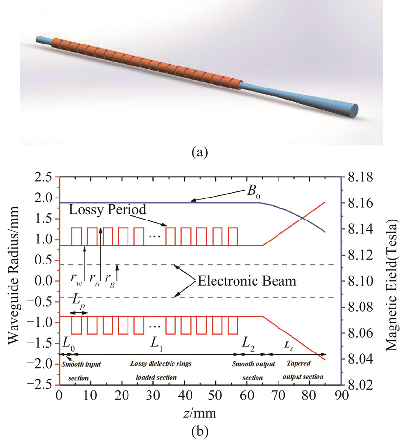
    Fig. 1. Beam-wave interaction circuit configurations of the 220 GHz Gyro-TWT (a) The 3-D structure diagram, (b) the interaction circuit schematic
    Dispersion diagram of 220 GHz PDL Gyro-TWT,(U0=70 kV,beam velocity pitch factor α=1.2,magnetic detuning ratio b=0.98. Point A,B,C are backward wave oscillation points. The red circular area is convective instability area)
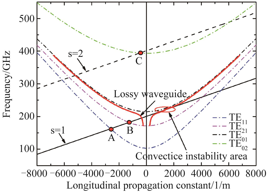
    Fig. 2. Dispersion diagram of 220 GHz PDL Gyro-TWT,(U0=70 kV,beam velocity pitch factor α=1.2,magnetic detuning ratio b=0.98. Point A,B,C are backward wave oscillation points. The red circular area is convective instability area)
    The coupling coefficient of 220 GHz PDL Gyro-TWT versus normalized guide center radius
    Fig. 3. The coupling coefficient of 220 GHz PDL Gyro-TWT versus normalized guide center radius
    The start current of absolute instability oscillation U0=70 kV, (a) losses circuit with different b, (b) lossy circuit with different conductance
    Fig. 4. The start current of absolute instability oscillation U0=70 kV, (a) losses circuit with different b, (b) lossy circuit with different conductance
    The start length of backward wave oscillations with voltage U0=70 kV and current I=3 A, (a) longitudinal field profiles in losses circuit, (b) start length changing versus different conductance
    Fig. 5. The start length of backward wave oscillations with voltage U0=70 kV and current I=3 A, (a) longitudinal field profiles in losses circuit, (b) start length changing versus different conductance
    The linear gain versus frequency with losses and different conductance lossy circuit(U0=70 kV,I=3 A,α=1.2,b=0.98)
    Fig. 6. The linear gain versus frequency with losses and different conductance lossy circuit(U0=70 kVI=3 Aα=1.2b=0.98
    The normalized field profiles of three backward wave oscillations in losses circuit(U0=70 kV,I=3 A,α=1.2,b=0.98)
    Fig. 7. The normalized field profiles of three backward wave oscillations in losses circuit(U0=70 kVI=3 Aα=1.2b=0.98
    At 220 GHz,U0=70 kV, I0=3 A, B=8.16 T, alpha=1.2,Pin=0.3 W,σ=58 S/m (a) the effect of the number of periods on the output power and gain, when Ld/Lp=0.83, (b) the effect of the dielectric slot ratio on the output power and gain when the number of periods is 21
    Fig. 8. At 220 GHz,U0=70 kV, I0=3 A, B=8.16 T, alpha=1.2,Pin=0.3 W,σ=58 S/m (a) the effect of the number of periods on the output power and gain, when Ld/Lp=0.83, (b) the effect of the dielectric slot ratio on the output power and gain when the number of periods is 21
    At 220 GHz,comparison of gain versus interaction circuit length(U0=70 kV,I0=3 A,B=8.16 T,alpha=1.2,Pin=0.55 W, and σ=58 S/m)
    Fig. 9. At 220 GHz,comparison of gain versus interaction circuit length(U0=70 kVI0=3 AB=8.16 Talpha=1.2Pin=0.55 W, and σ=58 S/m
    Pbeam,Pout and Ploss versus interaction circuit length(U0=70 kV,I0=3 A,B=8.16 T,alpha=1.2,Pin=0.3 W and σ=58 S/m,at 220 GHz)
    Fig. 10. PbeamPout and Ploss versus interaction circuit length(U0=70 kVI0=3 AB=8.16 Talpha=1.2Pin=0.3 W and σ=58 S/m,at 220 GHz)
    The TE11 backward wave oscillation phenomenon (with TE01 as input signal at 220 GHz, U0=70 kV, I0=3 APin=0.55 WL0=4.5 mm, L1=36 mm, L2=9.5 mm, εr=11-4.4 J,ro-rw=0.3 mm) (a) evolution of the quadratic root value of Ppeak in the output part versus time (b) frequency spectrum of the output signals
    Fig. 11. The TE11 backward wave oscillation phenomenon (with TE01 as input signal at 220 GHz, U0=70 kV, I0=3 APin=0.55 WL0=4.5 mm, L1=36 mm, L2=9.5 mm, εr=11-4.4 J,ro-rw=0.3 mm) (a) evolution of the quadratic root value of Ppeak in the output part versus time (b) frequency spectrum of the output signals
    Attenuation of dielectric versus the dielectric thickness with εr=11-4.4 J
    Fig. 12. Attenuation of dielectric versus the dielectric thickness with εr=11-4.4 J
    The TE21 backward wave oscillation phenomenon (with TE01 as input signal at 220 GHz, U0=70 kV, I0=3 APin=0.55 WL0=4.5 mm, L1=36 mm, L2=10.2 mmεr=11-4.4 Jro-rw=0.43 mm) (a) evolution of the quadratic root value of Ppeak in the output part versus time, (b) frequency spectrum of the output signals
    Fig. 13. The TE21 backward wave oscillation phenomenon (with TE01 as input signal at 220 GHz, U0=70 kV, I0=3 APin=0.55 WL0=4.5 mm, L1=36 mm, L2=10.2 mmεr=11-4.4 Jro-rw=0.43 mm) (a) evolution of the quadratic root value of Ppeak in the output part versus time, (b) frequency spectrum of the output signals
    Output port signal of the four mainly competitional modes versus the simulation time at zero drive
    Fig. 14. Output port signal of the four mainly competitional modes versus the simulation time at zero drive
    The 3D-PIC simulation results of optimized model (Pin=0.55 W, at 220 GHz) (a) evolution of the quadratic root value of Ppeak in the output port versus time, (b) frequency spectrum of the output signals
    Fig. 15. The 3D-PIC simulation results of optimized model (Pin=0.55 W, at 220 GHz) (a) evolution of the quadratic root value of Ppeak in the output port versus time, (b) frequency spectrum of the output signals
    Comparison of output power versus frequency with Pin=0.55 W at 220 GHz
    Fig. 16. Comparison of output power versus frequency with Pin=0.55 W at 220 GHz
    Comparison of output power gain versus Pin at 220 GHz
    Fig. 17. Comparison of output power gain versus Pin at 220 GHz
    ParametersSpecifications
    Beam voltage U070 kV
    Beam current I03 A
    Velocity pitch factor α1.2
    Waveguide radius rw0.85 mm
    Dielectric thickness(ro-rw0.43 mm
    Guiding center radius rg0.46*rw
    Operating modeTE01
    Dielectric property(Beo-Sic)11∼4.4 J
    Operating magnetic field B08.16 T
    Structure length L0L1L24.5 mm,50.4 mm,9.5 mm
    Dielectric slot ratioLd/Lp0.83
    Period lengthLp2.4 mm
    Table 1. Design parameters of 220 GHz Gyro-TWT
    Ru-Tai CHEN, Sheng YU. Theoretical study and PIC simulation of a 220 GHz Gyro-TWT with periodic dielectric loaded waveguide[J]. Journal of Infrared and Millimeter Waves, 2022, 41(6): 1042
    Download Citation