• Photonics Research
  • Vol. 10, Issue 7, 1731 (2022)
Shoujun Zhang1, Xieyu Chen1, Kuan Liu2, Haiyang Li2, Yuehong Xu1, Xiaohan Jiang1, Yihan Xu1, Qingwei Wang1, Tun Cao2、4、*, and Zhen Tian1、3、5、*
Author Affiliations
  • 1Center for Terahertz Waves and College of Precision Instrument and Optoelectronics Engineering, Key Laboratory of Optoelectronic Information Technology (Ministry of Education of China), Tianjin University, Tianjin 300072, China
  • 2School of Optoelectronic Engineering and Instrumentation Science, Dalian University of Technology, Dalian 116024, China
  • 3Georgia Tech Shenzhen Institute (GTSI), Tianjin University, Shenzhen 518067, China
  • 4e-mail: caotun1806@dlut.edu.cn
  • 5e-mail: tianzhen@tju.edu.cn
  • show less
    DOI: 10.1364/PRJ.456161 Cite this Article Set citation alerts
    Shoujun Zhang, Xieyu Chen, Kuan Liu, Haiyang Li, Yuehong Xu, Xiaohan Jiang, Yihan Xu, Qingwei Wang, Tun Cao, Zhen Tian. Nonvolatile reconfigurable dynamic Janus metasurfaces in the terahertz regime[J]. Photonics Research, 2022, 10(7): 1731 Copy Citation Text show less
    Operation principle of dynamic Janus metasurface. (a) Schematic demonstration of a nonvolatile reconfigurable Janus metasurface consisting of three sets of structures, U1, U2, and U3. Green, lilac, and gray structures are metallic CRs, amorphous G-CRs, and crystalline G-CRs, respectively. Incident THz waves are y-polarization, and cross-polarization transmitted waves are detected. Any two functionalities can be switched reversibly by recrystallization and reamorphization. Inset shows enlarged views of U1, U2, and U3. In active structures U1 and U2, there is an additional layer of GST between the Al CRs and the silicon substrate. (b) Schematic view of a single CR: Px=Py=80 μm is the period, r is the outer ring radius, w is the line width, α is the opening angle, and β is the orientation angle. (c) Simulated amplitude and phase shift of eight CRs at 0.8 THz. Geometrical parameters of the former four CRs are r=37,37,38,38 μm, w=8,15,9,5 μm, and α=120°,40°,30°,12°, respectively, with the same rotation angle β=45°. Another four structures can be obtained by mirroring along the y axis.
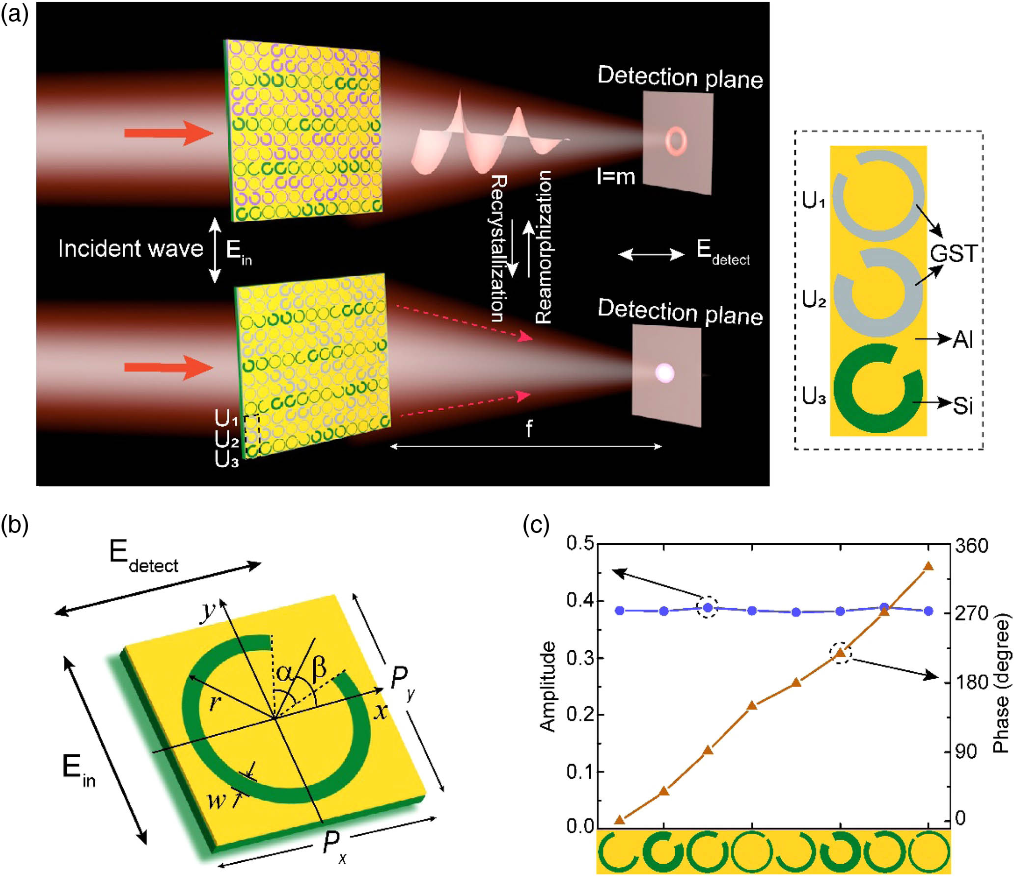
    Fig. 1. Operation principle of dynamic Janus metasurface. (a) Schematic demonstration of a nonvolatile reconfigurable Janus metasurface consisting of three sets of structures, U1, U2, and U3. Green, lilac, and gray structures are metallic CRs, amorphous G-CRs, and crystalline G-CRs, respectively. Incident THz waves are y-polarization, and cross-polarization transmitted waves are detected. Any two functionalities can be switched reversibly by recrystallization and reamorphization. Inset shows enlarged views of U1, U2, and U3. In active structures U1 and U2, there is an additional layer of GST between the Al CRs and the silicon substrate. (b) Schematic view of a single CR: Px=Py=80  μm is the period, r is the outer ring radius, w is the line width, α is the opening angle, and β is the orientation angle. (c) Simulated amplitude and phase shift of eight CRs at 0.8 THz. Geometrical parameters of the former four CRs are r=37,37,38,38  μm, w=8,15,9,5  μm, and α=120°,40°,30°,12°, respectively, with the same rotation angle β=45°. Another four structures can be obtained by mirroring along the y axis.
    Dynamic beam steering. (a) Schematic principle of the proposed dynamic beam splitter, which can steer cross-polarization THz waves toward two opposite directions in crystalline and amorphous states. (b) Optical microscope image of part of the fabricated metasurface and enlarged views of basic elements. The sample is composed of three sets of structures: U1, U2, and U3. The area of the fabricated metasurface is 5120 μm×5120 μm. (c), (e) Measured normalized intensity distribution as a function of deflection angle and frequency. By applying a single pulse with 120 mJ/cm2, the GST is transited from crystalline to amorphous state, and recrystallization of GST is realized by thermally annealing the sample at 300°C for 2 min on a hot plate. (d), (f) Corresponding normalized intensity profiles at 0.8 THz extracted from (c) and (e). (g) Experimentally measured and theoretically calculated deflection angles at various frequencies.
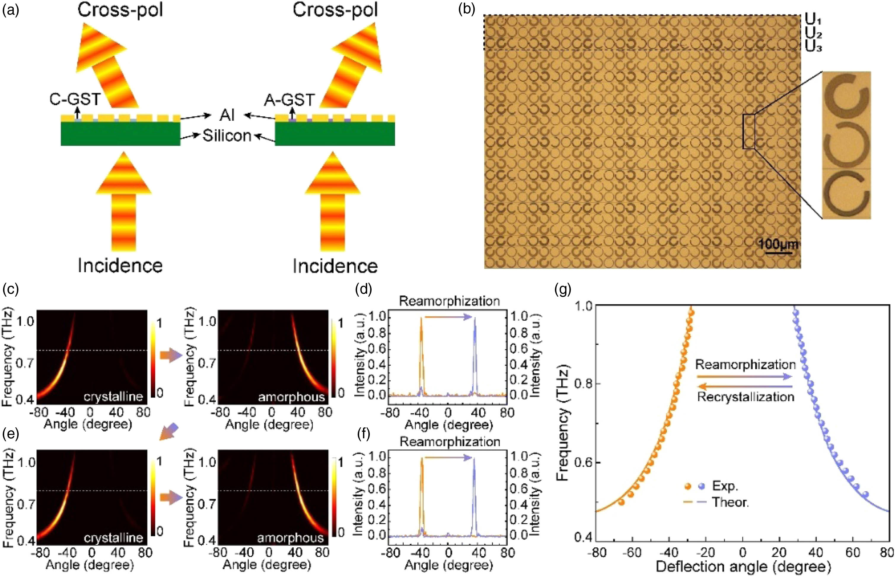
    Fig. 2. Dynamic beam steering. (a) Schematic principle of the proposed dynamic beam splitter, which can steer cross-polarization THz waves toward two opposite directions in crystalline and amorphous states. (b) Optical microscope image of part of the fabricated metasurface and enlarged views of basic elements. The sample is composed of three sets of structures: U1, U2, and U3. The area of the fabricated metasurface is 5120  μm×5120  μm. (c), (e) Measured normalized intensity distribution as a function of deflection angle and frequency. By applying a single pulse with 120  mJ/cm2, the GST is transited from crystalline to amorphous state, and recrystallization of GST is realized by thermally annealing the sample at 300°C for 2 min on a hot plate. (d), (f) Corresponding normalized intensity profiles at 0.8 THz extracted from (c) and (e). (g) Experimentally measured and theoretically calculated deflection angles at various frequencies.
    Dynamic bifocal metalens. (a) Schematic principle of the proposed dynamic bifocal metalens, which exhibits switchable focal lengths in amorphous and crystalline states of GST. (b) Optical microscope image of part of the fabricated metasurface and enlarged views of basic elements. The sample is composed of three sets of structures: U1, U2, and U3. The radius of the fabricated metasurface is 5120 μm. Measured normalized (c), (e), (g) x−z and (d), (f), (h) x−y plane electric field distributions in amorphous, crystalline, and reamorphization states of GST, respectively. Extracted THz intensity distributions along the (i) propagation direction and (j) y direction from (c), (e), (g) and (d), (f), (h).
    Fig. 3. Dynamic bifocal metalens. (a) Schematic principle of the proposed dynamic bifocal metalens, which exhibits switchable focal lengths in amorphous and crystalline states of GST. (b) Optical microscope image of part of the fabricated metasurface and enlarged views of basic elements. The sample is composed of three sets of structures: U1, U2, and U3. The radius of the fabricated metasurface is 5120 μm. Measured normalized (c), (e), (g) xz and (d), (f), (h) xy plane electric field distributions in amorphous, crystalline, and reamorphization states of GST, respectively. Extracted THz intensity distributions along the (i) propagation direction and (j) y direction from (c), (e), (g) and (d), (f), (h).
    Dual-mode FOV generator. (a) Schematic principle of dual-mode FOV generator, which exhibits different values of topological charge in amorphous and crystalline states of GST. (b) Optical microscope image of part of the fabricated metasurface and enlarged views of basic elements. The radius of the fabricated metasurface is 5120 μm. Measured normalized intensity distribution of (c)–(e) x−z and (f)–(h) x−y planes in amorphous, crystalline, and reamorphization states of GST, respectively. (i)–(k) Corresponding phase profiles are shown in black dotted lines.
    Fig. 4. Dual-mode FOV generator. (a) Schematic principle of dual-mode FOV generator, which exhibits different values of topological charge in amorphous and crystalline states of GST. (b) Optical microscope image of part of the fabricated metasurface and enlarged views of basic elements. The radius of the fabricated metasurface is 5120 μm. Measured normalized intensity distribution of (c)–(e) xz and (f)–(h) xy planes in amorphous, crystalline, and reamorphization states of GST, respectively. (i)–(k) Corresponding phase profiles are shown in black dotted lines.
    Dual-functionality metasurface. (a) Schematic principle of dual-functionality metasurface, which functions as an FOV generator in the amorphous state and as a metalens in the crystalline state of GST. (b) Optical microscope image of part of the fabricated metasurface and enlarged views of basic elements. The radius of the fabricated metasurface is 5120 μm. (c)–(e) Measured normalized intensity distributions of x−y planes at a height of 8.8 mm above the sample in amorphous, crystalline, and reamorphization states, respectively. (f)–(h) Corresponding phase profiles.
    Fig. 5. Dual-functionality metasurface. (a) Schematic principle of dual-functionality metasurface, which functions as an FOV generator in the amorphous state and as a metalens in the crystalline state of GST. (b) Optical microscope image of part of the fabricated metasurface and enlarged views of basic elements. The radius of the fabricated metasurface is 5120 μm. (c)–(e) Measured normalized intensity distributions of xy planes at a height of 8.8 mm above the sample in amorphous, crystalline, and reamorphization states, respectively. (f)–(h) Corresponding phase profiles.
    (a) Transmission at 0.8 THz of the same GST sample during multiple switching cycles. Inset: atom distribution diagrams of the two phases of GST. (b) Calculated conductivities in amorphous and crystalline states of GST.
    Fig. 6. (a) Transmission at 0.8 THz of the same GST sample during multiple switching cycles. Inset: atom distribution diagrams of the two phases of GST. (b) Calculated conductivities in amorphous and crystalline states of GST.
    (a) Simulated amplitude and phase shift of eight G-CRs in the amorphous state and amplitude in the crystalline state of GST at 0.8 THz. (b) Simulated amplitude and phase shift of eight CRs. The orientation angles of the former four CRs, β=30°, and another four structures are obtained by rotating 90° widdershins.
    Fig. 7. (a) Simulated amplitude and phase shift of eight G-CRs in the amorphous state and amplitude in the crystalline state of GST at 0.8 THz. (b) Simulated amplitude and phase shift of eight CRs. The orientation angles of the former four CRs, β=30°, and another four structures are obtained by rotating 90° widdershins.
    (a), (h) Optical microscope image of part of the fabricated metasurface and enlarged views of basic elements. The radius of the fabricated metasurface is 5120 μm. (b)–(d), (i)–(k) Measured normalized intensity distributions of x−y planes in amorphous, crystalline, and reamorphization states of GST, respectively. (e)–(g), (l)–(n) Corresponding phase profiles are shown in black dotted lines.
    Fig. 8. (a), (h) Optical microscope image of part of the fabricated metasurface and enlarged views of basic elements. The radius of the fabricated metasurface is 5120 μm. (b)–(d), (i)–(k) Measured normalized intensity distributions of xy planes in amorphous, crystalline, and reamorphization states of GST, respectively. (e)–(g), (l)–(n) Corresponding phase profiles are shown in black dotted lines.
    Broadband splitting ratios in both states of GST.
    Fig. 9. Broadband splitting ratios in both states of GST.
    Calculated purity of different vortex beams.
    Fig. 10. Calculated purity of different vortex beams.
    Shoujun Zhang, Xieyu Chen, Kuan Liu, Haiyang Li, Yuehong Xu, Xiaohan Jiang, Yihan Xu, Qingwei Wang, Tun Cao, Zhen Tian. Nonvolatile reconfigurable dynamic Janus metasurfaces in the terahertz regime[J]. Photonics Research, 2022, 10(7): 1731
    Download Citation