• Journal of Semiconductors
  • Vol. 40, Issue 1, 011804 (2019)
Bo Fu, Zhitai Jia, Wenxiang Mu, Yanru Yin, Jian Zhang, and Xutang Tao
Author Affiliations
  • State Key Laboratory of Crystal Materials & Key Laboratory of Functional Crystal Materials and Device, Shandong University, Jinan 250100, China
  • show less
    DOI: 10.1088/1674-4926/40/1/011804 Cite this Article
    Bo Fu, Zhitai Jia, Wenxiang Mu, Yanru Yin, Jian Zhang, Xutang Tao. A review of β-Ga2O3 single crystal defects, their effects on device performance and their formation mechanism[J]. Journal of Semiconductors, 2019, 40(1): 011804 Copy Citation Text show less
    (Color online) Monoclinic unit cell of β-Ga2O3 and relative lattice parameters.
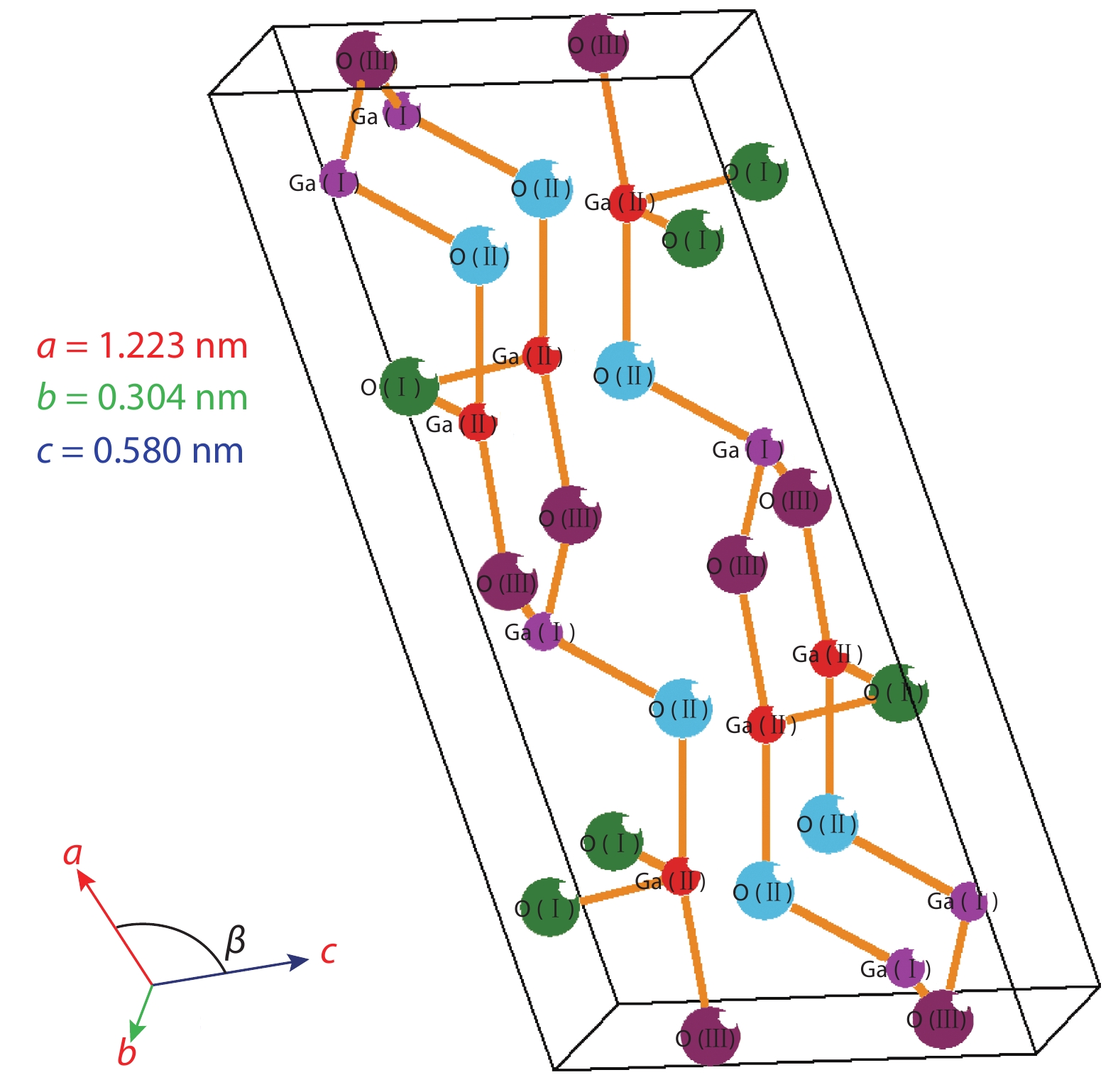
    Fig. 1. (Color online) Monoclinic unit cell of β-Ga2O3 and relative lattice parameters.
    (Color online) Bulk β-Ga2O3 crystals obtained by the following melt methods: (a) EFG, (b) VB, (c) Czochralski, and (d) OFZ. Copyright 2017 ECS Journal of Solid State Science and Technology[28]. Copyright 2016 J Cryst Growth[13]. Copyright 2014 J Cryst Growth[47]. Copyright 2004 J Cryst Growth[11].
    Fig. 2. (Color online) Bulk β-Ga2O3 crystals obtained by the following melt methods: (a) EFG, (b) VB, (c) Czochralski, and (d) OFZ. Copyright 2017 ECS Journal of Solid State Science and Technology[28]. Copyright 2016 J Cryst Growth[13]. Copyright 2014 J Cryst Growth[47]. Copyright 2004 J Cryst Growth[11].
    (Color online) Theoretical limits of on-resistance versus breakdown voltage in unipolar power devices for β-Ga2O3 and other major semiconductors. Copyright 2014 Physical Status Solidi[29].
    Fig. 3. (Color online) Theoretical limits of on-resistance versus breakdown voltage in unipolar power devices for β-Ga2O3 and other major semiconductors. Copyright 2014 Physical Status Solidi[29].
    Cross-sectional TEM image of a dislocation viewed from []. Copyright 2015 Jpn J Appl Phys[38].
    Fig. 4. Cross-sectional TEM image of a dislocation viewed from [ ]. Copyright 2015 Jpn J Appl Phys[38].
    (Color online) (a) Optical micrograph of surface of () plane after etching. (b) Enlarged image of the etch pits. An XTEM sample is indicated by a white line. Copyright 2016 Jpn J Appl Phys[39].
    Fig. 5. (Color online) (a) Optical micrograph of surface of ( ) plane after etching. (b) Enlarged image of the etch pits. An XTEM sample is indicated by a white line. Copyright 2016 Jpn J Appl Phys[39].
    Cross-sectional TEM image of a hollow nanopipes defect viewed from []. Copyright 2015 Jpn J Appl Phys[38].
    Fig. 6. Cross-sectional TEM image of a hollow nanopipes defect viewed from [ ]. Copyright 2015 Jpn J Appl Phys[38].
    (a) A cross-sectional FIB-SIM image of an PNPs defects. Copyright 2016 Jpn J Appl Phys[39]. (b) SEM image of three NSGs in an array along the [001] direction. Copyright 2016 Jpn J Appl Phys[40].
    Fig. 7. (a) A cross-sectional FIB-SIM image of an PNPs defects. Copyright 2016 Jpn J Appl Phys[39]. (b) SEM image of three NSGs in an array along the [001] direction. Copyright 2016 Jpn J Appl Phys[40].
    (Color online) DICM images showing line-shaped voids exposed on the surface etching for (a) 5 min and (b) 25 min. (c) Length histogram of the 625 line-shaped voids observed on the 5-min etched surface. Copyright 2017 Jpn J Appl Phys[44].
    Fig. 8. (Color online) DICM images showing line-shaped voids exposed on the surface etching for (a) 5 min and (b) 25 min. (c) Length histogram of the 625 line-shaped voids observed on the 5-min etched surface. Copyright 2017 Jpn J Appl Phys[44].
    (a) An SEM image of etched surface of () plane including a twin boundary. (b) The atomic structure of a region including a twin lamellae in β-Ga2O3 crystal viewed from the () direction. Copyright 2016 Jpn J Appl Phys[39].
    Fig. 9. (a) An SEM image of etched surface of ( ) plane including a twin boundary. (b) The atomic structure of a region including a twin lamellae in β-Ga2O3 crystal viewed from the ( ) direction. Copyright 2016 Jpn J Appl Phys[39].
    (Color online) AFM images of an arrow-shaped etch pit. Copyright 2017 Jpn J Appl Phys[45].
    Fig. 10. (Color online) AFM images of an arrow-shaped etch pit. Copyright 2017 Jpn J Appl Phys[45].
    (Color online) AFM image of a gourd-shaped etch pit. Copyright 2017 Jpn J Appl Phys[45].
    Fig. 11. (Color online) AFM image of a gourd-shaped etch pit. Copyright 2017 Jpn J Appl Phys[45].
    SEM images of six etch pits of different shapes (Types A, B, C, D, E, and F) according to shapes of the etch pits on β-Ga2O3 (010) single crystal surface. Copyright 2016 Jpn J Appl Phys.[43]
    Fig. 12. SEM images of six etch pits of different shapes (Types A, B, C, D, E, and F) according to shapes of the etch pits on β-Ga2O3 (010) single crystal surface. Copyright 2016 Jpn J Appl Phys.[43]
    SEM images of the same pit at the same position on the same β-Ga2O3 (010) single crystal surface etched for the etching times of 0, 2, 4, and 10 min. Copyright 2016 Jpn J Appl Phys[43].
    Fig. 13. SEM images of the same pit at the same position on the same β-Ga2O3 (010) single crystal surface etched for the etching times of 0, 2, 4, and 10 min. Copyright 2016 Jpn J Appl Phys[43].
    (Color online) (a) Distributions of number of dislocations and reverse leakage current (IR) in SBD. (b) Distributions of number of dislocations and forward leakage current (IF) in SBDs. (c) Distributions of number of voids and reverse leakage current (IR) in SBDs. (d) Distributions of number of voids and forward leakage current (IF) in SBDs. Copyright 2016 Jpn J Appl Phys[48].
    Fig. 14. (Color online) (a) Distributions of number of dislocations and reverse leakage current (IR) in SBD. (b) Distributions of number of dislocations and forward leakage current (IF) in SBDs. (c) Distributions of number of voids and reverse leakage current (IR) in SBDs. (d) Distributions of number of voids and forward leakage current (IF) in SBDs. Copyright 2016 Jpn J Appl Phys[48].
    (a) Relationship between the reverse leakage current and the number of arrow-shaped etch pits in SBD. (b) Relationship between the reverse leakage current and the number of gourd-shaped etch pits in SBD. The area of each SBD (S) is 1 × 10⁻³ cm2. Copyright 2017 Jpn J Appl Phys[45].
    Fig. 15. (a) Relationship between the reverse leakage current and the number of arrow-shaped etch pits in SBD. (b) Relationship between the reverse leakage current and the number of gourd-shaped etch pits in SBD. The area of each SBD (S) is 1 × 10⁻³ cm2. Copyright 2017 Jpn J Appl Phys[45].
    Schematic of a subgrain boundary. Copyright 2015 Jpn J Appl Phys[38].
    Fig. 16. Schematic of a subgrain boundary. Copyright 2015 Jpn J Appl Phys[38].
    ParameterEdge dislocationScrew dislocationTwinHollow nanopipesPNPsNSGsLine-shaped grooves
    Crystal plane( ) (010)( ) (010)(010)(010)( )(001)
    Crystal direction//[010]//[100]//[102]No direction//[100]//[001]No direction
    Dislocation directionNot exactly normal to ( ) but slightly tilting to [102] //[010]
    Burgers vector//[010]//[010]
    Twin plane(100)
    Void direction//[010]//[010]//[010]//[010]
    Table 1. All kinds of defects observed on different β-Ga2O3 crystal plane.
    Bo Fu, Zhitai Jia, Wenxiang Mu, Yanru Yin, Jian Zhang, Xutang Tao. A review of β-Ga2O3 single crystal defects, their effects on device performance and their formation mechanism[J]. Journal of Semiconductors, 2019, 40(1): 011804
    Download Citation