
Bo Fu, Zhitai Jia, Wenxiang Mu, Yanru Yin, Jian Zhang, Xutang Tao. A review of β-Ga2O3 single crystal defects, their effects on device performance and their formation mechanism[J]. Journal of Semiconductors, 2019, 40(1): 011804
- Journal of Semiconductors
- Vol. 40, Issue 1, 011804 (2019)
Abstract
1. Introduction
Recently, β-Ga2O3 has attracted great attention as an ultra wide band-gap oxide semiconductor for future power and photodetector devices. In order to achieve high-performance and high-reliability of semiconductor devices, it is critical to control crystal defects because those defects could have negative and damaging effects on the device performance. In some cases, those crystal defects can even bring about leakage current and lower breakdown voltage, such as micropipes observed in SiC. Thus, it is essential to characterize defects in the crystal and understand their formation mechanism.
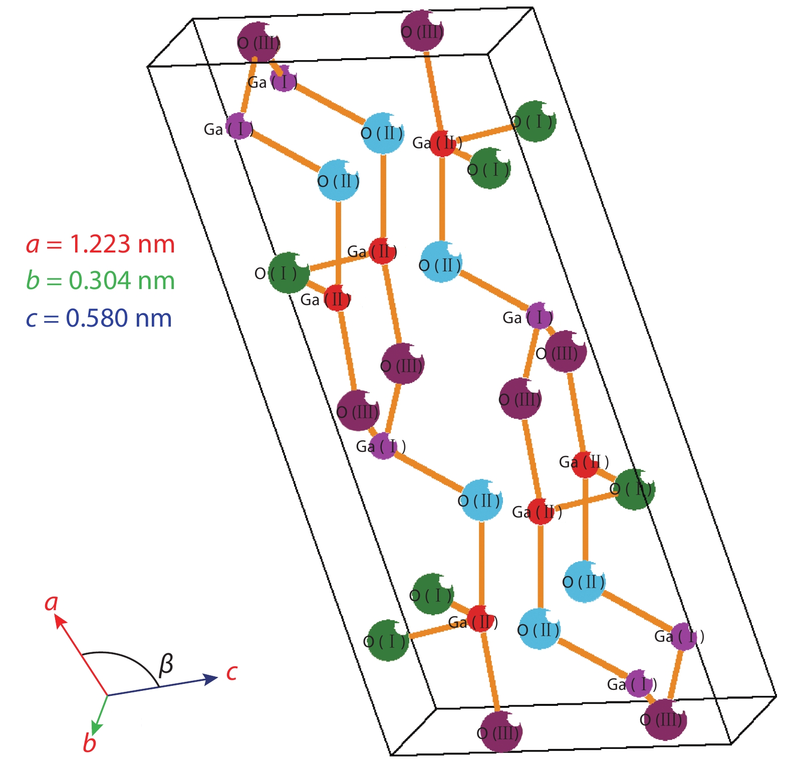
The crystal structure of β-Ga2O3 is shown in Fig. 1. β-Ga2O3 is the most thermodynamically stable one in terms of the six different phases of the α, β, γ, δ, ε, and φ phases[
![]()
Figure 1.(Color online) Monoclinic unit cell of
The melting point of Ga2O3 is approximately 1800 °C[
Fig. 2 showed the examples of bulk β-Ga2O3 single crystals obtained by melt growth methods: (a) EFG, (b) VB, (c) Czochralski and (d) OFZ. The EFG method employs a die or a shaper that is placed in a metal crucible. The melt is transported from the crucible to a shaped top surface of the die by a narrow slit or channel due to capillary forces. The growth direction is always along the [010] crystallographic direction, which is paralleled to both cleavage planes (100) and (001). Presently, the EFG method is able to fabricate substrate of 2″ (commercialized), 4″ (demonstrated), and possible 6″ (under research & development) as shown in Fig. 2(a). The VB method utilizing a Pt-Rh (70%–30%) alloy crucible to grow β-Ga2O3 single crystal is in development, which is favorable for high oxygen concentration. The crystal of 25 mm in diameter is grown in air without a crystal seed as shown in Fig. 2(b). As for the crystal growth by Czochralski method, crystal spiral growth turns out to be the main challenge. However, the novel approach with a CO2-containing growth atmosphere providing oxygen partial pressures, allows to obtain 2″ in diameter crystals as shown in Fig. 2(c). The OFZ method is a crucible-free technique. The main advantage of this method is the possibility of using highly oxidizing atmosphere to suppress the volatilization of β-Ga2O3. Crystals with 1 in. diameter have been reported as shown in Fig. 2(d).
![]()
Figure 2.(Color online) Bulk
β-Ga2O3 has attracted much interest as a substrate to grow GaN heteroepitaxy for efficient high-brightness vertically-structured LEDs due to its good conductivity and nice transparency[
![]()
Figure 3.(Color online) Theoretical limits of on-resistance versus breakdown voltage in unipolar power devices for
In this review, we summarize all kinds of defects observed in β-Ga2O3 single crystal recently. Subsequently, the effects of defects on device performance and their formation mechanism are summarized and analyzed in detail, which will provide a basis reference for device performance improvement in the future.
2. Four types of defects in β-Ga2O3 single crystal
2.1. Dislocations
The dislocations can be divided into two types, screw dislocation and edge dislocation. Nakai et al. found out the screw dislocations on the (010) plane[
![]()
Figure 4.Cross-sectional TEM image of a dislocation viewed from [
Ueda et al. reported the edge dislocation on the (
![]()
Figure 5.(Color online) (a) Optical micrograph of surface of (
2.2. Voids
The voids defect has some volume, and thus can be observed on different crystal planes, including hollow nanopipes[
![]()
Figure 6.Cross-sectional TEM image of a hollow nanopipes defect viewed from [
A very narrow groove[
![]()
Figure 7.(a) A cross-sectional FIB-SIM image of an PNPs defects. Copyright 2016 Jpn J Appl Phys[
Numerous line-shaped grooves[
![]()
Figure 8.(Color online) DICM images showing line-shaped voids exposed on the surface etching for (a) 5 min and (b) 25 min. (c) Length histogram of the 625 line-shaped voids observed on the 5-min etched surface. Copyright 2017 Jpn J Appl Phys[
2.3. Twin
A large number of defects were reported on (010), (001), and (
![]()
Figure 9.(a) An SEM image of etched surface of (
2.4. Small defects
Apart from the mentioned defects above, small defects were also found. However, the small defects exist in the shape of different types of etch pits, including arrow-shaped etch pit[
![]()
Figure 10.(Color online) AFM images of an arrow-shaped etch pit. Copyright 2017 Jpn J Appl Phys[
Fig. 11 showed the AFM image of a gourd-shaped etch pit. The point head faced toward the [102] direction. The average density was 9 × 104 cm−2. The depth of the gourd-shaped etch pit was 25 nm, which was much less than that of the arrow-shaped etch pit (600 nm). Thus, the gourd-shaped etch pit tended to be shallower than the arrow-shaped etch pit. Some gourd-shaped etch pits also tended to form an array along the [010] direction. The origin of the gourd-shaped etch pit should be a dislocation similar to the arrow-shaped etch pit.
![]()
Figure 11.(Color online) AFM image of a gourd-shaped etch pit. Copyright 2017 Jpn J Appl Phys[
Furthermore, Hanada et al.[
![]()
Figure 12.SEM images of six etch pits of different shapes (Types A, B, C, D, E, and F) according to shapes of the etch pits on
![]()
Figure 13.SEM images of the same pit at the same position on the same
2.5. Defects summary
Table 1 covers all types of defects, except small defects [discussed in 3.2], observed on different β-Ga2O3 crystal planes. Actually, in terms of defects features, these defects can be classified into three types: (1) dislocation (edge dislocation and screw dislocation),(2) defects that originated from voids (hollow nanopipes, PNPs, NSGs, line-shaped grooves), (3) twin. The Burgers vector of edge and screw dislocation observed on (
3. Effects of the defects on device performance and their formation mechanism
3.1. Effects of the defects on device performance
In this section, four types of defects have been found in β-Ga2O3, and their effects on device performance are to be summarized. The effects on device performances caused by dislocation and void have been discussed by Kasu et al.[
Fig. 14(c) showed the relationship between the number of void etch pits and the reverse leakage current (IR). The number of voids was represented by the diameter of the circle. The black, yellow, and red circles represented low, intermediate, and high reverse leakage currents (IR), respectively. The SBDs in the lower left-hand region showed a large number of voids and a high leakage current. Therefore, the void defects in this region produced a leakage current.
In addition, on the right-hand side, SBDs with large number of dislocations showed a low reverse leakage current (black circles) in the Fig. 14(c). The void defects in this region, however, did not produce leakage current. Therefore, it seemed that not all void-type defects produce a leakage current. At present, it can be confirmed that voids were terminated within the crystal[
![]()
Figure 14.(Color online) (a) Distributions of number of dislocations and reverse leakage current (
It is common knowledge that dislocation only terminates on crystal surface or boundary. In other words, once the dislocation is formed, it goes through the whole crystal plate easily. Subsequently, dislocation and the surrounding regions will act as paths for the leakage current of SBD in single crystal. However, not all voids produce leakage current. It not only depends on the orientation relationship between the extending direction of the void and the crystal plane, but also on the length of the void. The line-shaped grooves observed on the (001) and (
Apart from the defects of dislocation and void, it was not confirmed whether arrow-shaped etch pits[
![]()
Figure 15.(a) Relationship between the reverse leakage current and the number of arrow-shaped etch pits in SBD. (b) Relationship between the reverse leakage current and the number of gourd-shaped etch pits in SBD. The area of each SBD (S) is 1 × 10⁻³ cm2. Copyright 2017 Jpn J Appl Phys[
In addition to the reported effects of dislocation on the leakage current for power device above, the dislocation in β-Ga2O3 single crystal may have other impacts on the electrical properties. The dislocation may generate a large number of electrically active centers due to the uncoordinated atoms in the dislocation core, which can lead to the formation of new energy levels in the band gap. In addition, the dislocation may also change parameters related to carriers, such as carrier lifetime and mobility, because it can become the capture center of carriers[
The effects of twin on electrical properties have not been reported up to now. However, the optical and electrical properties of β-Ga2O3 single crystal, such as photoabsorption and carrier characteristics, may change due to the existence of twin[
3.2. The formation mechanism of defects
It is of great importance to improve the quality of crystals by clarifying the formation mechanism of the defects, in order that they may provide adequate support for device performance. In Section 2.5, the defects observed in β-Ga2O3 crystal were divided into three types: dislocation, void and twin. However, the small defects, including the arrow-shaped and gourd-shaped etch pits, were not regarded as intrinsic defects. It is well known that the crystal plate must be polished before etching. Presently, chemical mechanic polishing (CMP) is very popular with wafer manufacture because it can cause little polishing scratch and mechanical damage compared with common mechanical polish. However, CMP also causes unintentional damage to wafers. Most small defects are induced by mechanical damages[
The dislocation can be induced by many conditions when growing bulk single crystal. The common case is that the dislocations existing in crystals are caused by the extension of defect from the seed to the grown crystal. In most cases, that can be eliminated by the technology of “neck”[
![]()
Figure 16.Schematic of a subgrain boundary. Copyright 2015 Jpn J Appl Phys[
where b was the magnitude of the Burgers vector and D was the spacing between dislocations. So far, they have no TEM results of the dislocations under etch pits aligning along [100]. However, the shape of the etch pits was similar to that aligning along [102]. Therefore, they supposed that the defects under etch pits aligning along [100] were also screw dislocations.
Edge dislocations lying on a plane slightly tilted towards the (102) plane, with a possible slip plane being the (101) plane, which has also been reported by Yamaguchi et al.[
Indeed, both PNPs and NSGs can be classified as hollow nanopipes. These hollow nanopipes have no surrounding strain field, therefore, the formation mechanism of them are different from the defects of micropipe observed in SiC. The micropipe is known to be hollow with a diameter of 2–3μm[
(1) The condensation of excess oxygen vacancies in the grown crystal generates multiple vacancy-type stacking faults on the crystal plane and finally forms voids.
(2) The voids are formed by the penetration of tiny bubbles at the liquid–solid interface into grain boundaries.
(3) The voids are formed by local meltback at some grown-in defects such as screw-type dislocations during growth.
Up to now, numerous experiments and tests are being done in order to clarify the generation mechanism of voids, but no conclusion has been drawn.
Referring to the crystal growth methods related to CZ, twins are typical defects that often generate in the early stage, namely, the shoulder part of the bulk crystals. It is also well known that twins are assumed to be generated by strain relaxation during the crystal growth, and they can be suppressed by adjusting the growth conditions. Twins are originated commonly from the TPB point (intersection of liquid-solid-gas)[
(1) The facet at the position of TPB point appears on the crystal surface.
(2) Special shoulder angle is required to form the twin on the external surface and make the facet exist continuously. At the same time, the contact angle between the growing surface and the meniscus surface makes the tension balanced at the TPB point exactly.
(3) There is a big degree of supercooling outside the crystal surface.
As for the twins observed in β-Ga2O3 crystal[
4. Conclusion
In this paper, we have presented four types of defects in β-Ga2O3 single crystal, discussed their effects on device performance and analyzed their formation mechanisms in detail.
Four types of defects, namely dislocations, voids, twin and small defects, were found in β-Ga2O3. The dislocations can be divided into two types, screw and edge dislocation. The hollow nanopipes, PNPs, NSGs and line-shaped grooves were originated from the voids defects. An important defect, twin, was observed on the (100) crystal plane.
The effects of those defects on device performance were also discussed. The dislocation and the surrounding regions can act as paths for the leakage current of SBD in single crystal. However, not all voids produced leakage current. It not only depended on the orientation relationship between the extending direction of the void and the crystal plane, but also on the length of the void. There’s no strong evidence yet to show that the etch-pitting method plays a role in proving small defects affect the electrical properties. In addition, doping impurity was definitely not related to the leakage current.
The formation mechanism of defects in β-Ga2O3 single crystal was analyzed in detail. Most of the small defects, such as the arrow-shaped and gourd-shaped etch pits, were induced by mechanical damages. The screw dislocation was originated from a subgrain boundary. The edge dislocation lying on a plane slightly tilted towards the (102) plane, with the (101) plane being the possible slip plane. The voids defect, including hollow nanopipes, PNPs, NSGs and line-shaped grooves may be caused by the condensation of excess oxygen vacancies, the penetration of tiny bubbles or local meltback. The nucleation of twin lamellae was formed at an initial stage of the “shoulder part” during the crystal growth.
These findings also suggest that the formation of defects can be controlled by adjusting the growth condition of the bulk crystal and the subsequent substrate fabrication process. Thus, it is hopeful to fabricate devices with better electrical performance on β-Ga2O3 single crystal.
Acknowledgment
We gratefully acknowledge the Financial support from the National key Research and Development Program of China (Nso. 2018YFB0406502,2016YFB1102201), the National Natural Science Foundation of China (Grant No.51321091), the key Research and Development Program of Shandong Province (No. 2018CXGC0410), the Young Scholars Program of Shandong University (No. 2015WLJH36), and the 111 Project 2.0 (No. BP2018013).
References
[1] M Baldini, Z Galazka, G Wagner. Recent progress in the growth of
[2] S J Pearton, J Yang, IV P H Cary et al. A review of Ga2O3 materials, processing, and devices. Appl Phys Rev, 5, 011301(2018).
[3] S Jang, S Jung, K Beers et al. A comparative study of wet etching and contacts on (2-01) and (010) oriented
[4]
[5] S I Stepanov, V I Nikolaev, V E Bougrov et al. Gallium oxide: properties and applica a review. Rev Adv Mater Sci, 44, 63(2016).
[6] T Harwig, G J Wubs, G J Dirksen. Electrical properties of
[7] A O Chase. Growth of
[8] M R Lorenz, J F Woods, R J Gambino. Some electrical properties of the semiconductor
[9] E G Víllora, M Yamaga, T Inoue et al. Optical spectroscopy study on
[10] J Zhang, B Li, C Xia et al. Growth and spectral characterization of
[11] E G Víllora, K Shimamura, Y Yoshikawa et al. Large-size
[12] E Ohba, T Kobayashi, M Kado et al. Defect characterization of
[13] K Hoshikawa, E Ohba, T Kobayashi et al. Growth of
[14] A Hideo, N Kengo, T Hidetoshi et al. Growth of
[15] R O Bell. Modeling of the time dependence of EFG crystal growth. J Cryst Growth, 104, 23(1990).
[16] L Braescu, T Duffar. Effect of buoyancy and Marangoni forces on the dopant distribution in a single crystal fiber grown from the melt by edge-defined film-fed growth (EFG) method. J Cryst Growth, 310, 484(2008).
[17] O Bunoiu, I Nicoara, J L Santailler et al. Fluid flow and solute segregation in EFG crystal growth process. J Cryst Growth, 275, e799(2005).
[18] Z Galazka, R Uecker, R Fornari. A novel crystal growth technique from the melt: levitation-assisted self-seeding crystal growth method. J Cryst Growth, 388, 61(2014).
[19] K Shimamura, E G Villora. Czochralski-Based growth and characteristics of selected novel single crystals for optical applications. Acta Phys Polon A, 124, 265(2013).
[20] Z Galazka, R Uecker, K Irmscher et al. Czochralski growth and characterization of
[21] K Irmscher, Z Galazka, M Pietsch et al. Electrical properties of
[22] Y Tomm, P Reiche, D Klimm et al. Czochralski grown Ga2O3 crystals. Jpn J Appl Phys, 220, 510(2000).
[23] Z Galazka, R Uecker, D Klimm et al. Scaling-up of bulk
[24] G Katz, R Roy. Flux Growth and characterization of
[25] V I Chani, K Inoue, K Shimamura et al. Segregation coefficients in
[26] T Matsumoto, M Aoki, A Kinoshita et al. Absorption and reflection of vapor grown single crystal platelets of
[27] H Juskowiak, A Pajaczkowska. Chemical transport of
[28] M A Mastro, A Kuramata, J Calkins et al. Perspective—opportunities and future directions for Ga2O3. ECS J Solid State Sci Technol, 6, 356(2017).
[29] M Higashiwaki, K Sasaki, A Kuramata et al. Development of gallium oxide power devices. Physl Status Solidi A, 211, 21(2014).
[30] K Shimamura, E G Víllora, K Domen et al. Epitaxial growth of GaN on (1 0 0)
[31] P J Wellmann. Power electronic semiconductor materials for automotive and energy saving applications–SiC, GaN, Ga2O3, and diamond. Zeitschrift für anorganische und allgemeine Chemie, 643, 1312(2017).
[32] M Higashiwaki, K Sasaki, A Kuramata et al. Gallium oxide (Ga2O3) metal–semiconductor field-effect transistors on single-crystal
[33] M Higashiwaki, K Sasaki, H Murakami et al. Recent progress in Ga2O3 power devices. Semicond Sci Technol, 31, 034001(2016).
[34] N Ma, N Tanen, A Verma et al. Intrinsic electron mobility limits in
[35] S Fujita. Wide-bandgap semiconductor materials: For their full bloom. Jpn J Appl Phys, 54, 030101(2015).
[36] R P Burns. Systematics of the evaporation coefficient Al2O3, Ga2O3, In2O3. J Chem Phys, 44, 3307(1966).
[37] J Takahashi, M Kanaya, Y Fujiwara. Sublimation growth of SiC single crystalline ingots on faces perpendicular to the (0001) basal plane. J Cryst Growth, 135, 61(1994).
[38] K Nakai, T Nagai, K Noami et al. Characterization of defects in
[39] O Ueda, N Ikenaga, K Koshi et al. Structural evaluation of defects in
[40] K Hanada, T Moribayashi, T Uematsu et al. Observation of nanometer-sized crystalline grooves in as-grown
[41] P G Neudeck, J A Powell. Performance limiting micropipe defects in silicon carbide wafers. IEEE Electron Device Lett, 15, 63(1994).
[42] M A Crimp, B A Simkin, B C Ng. Demonstration of the g· bxu = 0 edge dislocation invisibility criterion for electron channelling contrast imaging. Philosophical Magazine Letters, 81, 833(2001).
[43] K Hanada, T Moribayashi, K Koshi et al. Origins of etch pits in
[44] T Oshima, A Hashiguchi, T Moribayashi et al. Electrical properties of Schottky barrier diodes fabricated on (001)
[45] M Kasu, T Oshima, K Hanada et al. Crystal defects observed by the etch-pit method and their effects on Schottky-barrier-diode characteristics on (-201)
[46] A Kuramata, K Koshi, S Watanabe et al. High-quality
[47] Z Galazka, K Irmscher, R Uecker et al. On the bulk
[48] M Kasu, K Hanada, T Moribayashi et al. Relationship between crystal defects and leakage current in
[49] L V C Assali. Electrically active centers in partial dislocations in semiconductors. Physica B, 308, 489(2001).
[50] I Capan, V Borjanović, B Pivac. Dislocation-related deep levels in carbon rich p-type polycrystalline silicon. Sol Energy Mater Sol Cells, 91, 931(2007).
[51] Z Ikonić, G P Srivastava, J C Inkson. Electronic properties of twin boundaries and twinning superlattices in diamond-type and zinc-blende-type semiconductors. Phys Rev B, 48, 17181(1993).
[52] H Yamaguchi, A Kuramata, T Masui. Slip system analysis and X-ray topographic study on
[53]
[54] F C Frank. Capillary equilibria of dislocated crystals. Acta Crystallographica, 4, 497(1951).
[55] W C Dash. Silicon crystals free of dislocations. J Appl Phys, 29, 736(1958).
[56] W C Dash. Improvements on the pedestal method of growing silicon and germanium crystals. J Appl Phys, 31, 736(1960).
[57] T Taishi, X Huang, I Yonenaga et al. Behavior of the edge dislocation propagating along the growth direction in Czochralski Si crystal growth. J Cryst Growth, 275, e2147(2005).
[58] T Taishi, Y Ohno, I Yonenaga et al. Influence of seed/crystal interface shape on dislocation generation in Czochralski Si crystal growth. Physica B, 401, 560(2007).
[59] J W Noor, B Dam. The growth spiral morphology on {100} KDP related to impurity effects and step kinetics. J Cryst Growth, 76, 243(1986).
[60]
[61] V V Chaldyshev, A L Kolesnikova, N A Bert et al. Investigation of dislocation loops associated with As–Sb nanoclusters in GaAs. J Appl Phys, 97, 024309(2005).
[62] M Neubert, A Kwasniewski, R Fornari. Analysis of twin formation in sphalerite-type compound semiconductors: A model study on bulk InP using statistical methods. J Cryst Growth, 310, 5270(2008).
[63] H Chung, M Dudley, D J Jr Larson et al. The mechanism of growth-twin formation in zincblende crystals: new insights from a study of magnetic liquid encapsulated Czochralski-grown InP single crystals. J Cryst Growth, 187, 9(1998).

Set citation alerts for the article
Please enter your email address
© Copyright 2018-2021 | Chinese Laser Press. All Rights Reserved 沪ICP备15018463号-20