• Laser & Optoelectronics Progress
  • Vol. 59, Issue 9, 0922016 (2022)
Shiguang Li1、2、3、†,*, Lei Guo1、2、3、†,**, Haifeng Zeng1、2、3, Yiyun Ji1、2、3, Yin Wang1、2、3, and Yanqing Xiao3
Author Affiliations
  • 1School of Integrated Circuits, University of Chinese Academy of Sciences, Beijing 100049, China
  • 2Achievement Transfer Department, Institute of Microelectronics, Chinese Academy of Sciences, Beijing 100029, China
  • 3Jiangsu Yingsu Integrated Circuit Equipment Co., Ltd., Xuzhou 221300, Jiangsu , China
  • show less
    DOI: 10.3788/LOP202259.0922016 Cite this Article Set citation alerts
    Shiguang Li, Lei Guo, Haifeng Zeng, Yiyun Ji, Yin Wang, Yanqing Xiao. Focus Control in Optical Lithography[J]. Laser & Optoelectronics Progress, 2022, 59(9): 0922016 Copy Citation Text show less
    Illustration of Ry
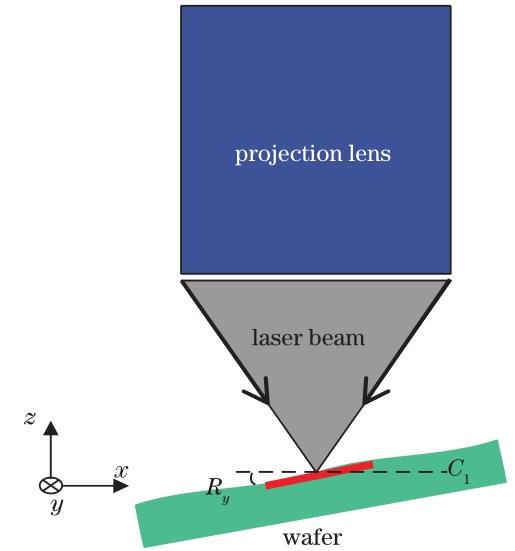
    Fig. 1. Illustration of Ry
    Probability distribution of the sum of non-normal distribution error (caused by Ry) and normal distribution error (stochastic error)
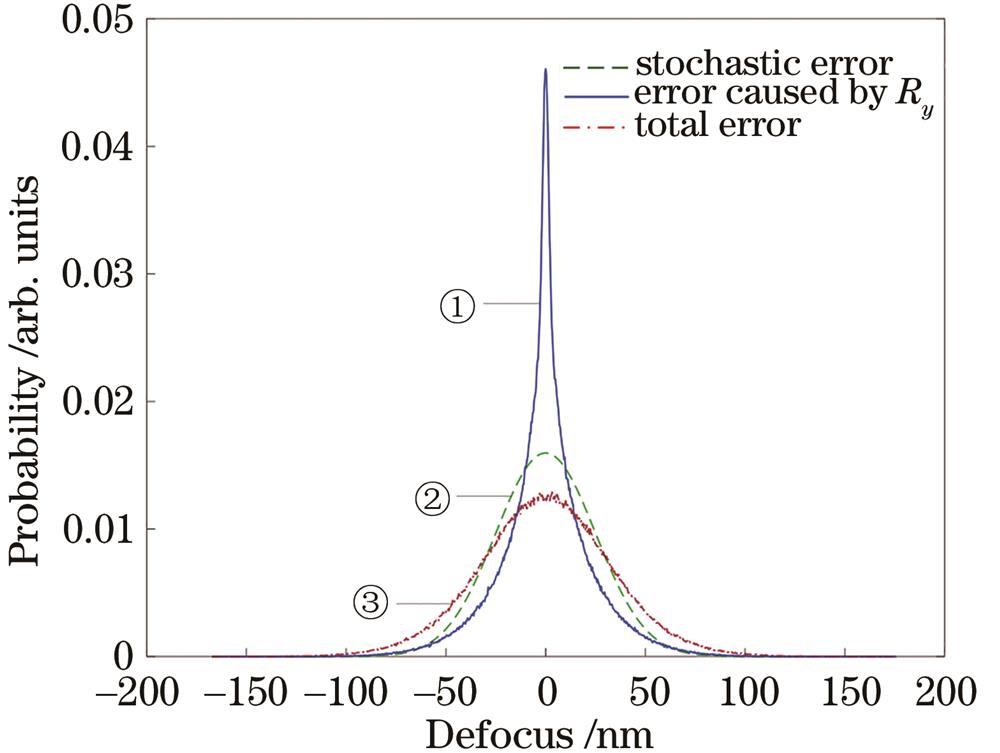
    Fig. 2. Probability distribution of the sum of non-normal distribution error (caused by Ry) and normal distribution error (stochastic error)
    Schematic diagram of the advanced lithographic architecture
    Fig. 3. Schematic diagram of the advanced lithographic architecture
    Focus control workflow of dual-stage lithographic system[10]
    Fig. 4. Focus control workflow of dual-stage lithographic system[10]
    DMD lithography system
    Fig. 5. DMD lithography system
    Work flow related to focus control in mask manufacturing process
    Fig. 6. Work flow related to focus control in mask manufacturing process
    Illustration of wafer surface measurement with optical triangulation method
    Fig. 7. Illustration of wafer surface measurement with optical triangulation method
    Canon’s early focusing and leveling sensor[14]
    Fig. 8. Canon’s early focusing and leveling sensor[14]
    Another Canon’s focusing and leveling sensor[15]
    Fig. 9. Another Canon’s focusing and leveling sensor[15]
    Detecting beams and optical spots on the wafer surface[15]
    Fig. 10. Detecting beams and optical spots on the wafer surface[15]
    Nikon’s focusing and leveling sensor[16]
    Fig. 11. Nikon’s focusing and leveling sensor[16]
    Light spot array produced through slits in Nikon’s focusing and leveling sensor[17]
    Fig. 12. Light spot array produced through slits in Nikon’s focusing and leveling sensor[17]
    Nikon’s focusing and leveling sensor equipped with reflecting prism[18]
    Fig. 13. Nikon’s focusing and leveling sensor equipped with reflecting prism[18]
    Lithography of Nikon. (a) Illustration; (b) corresponding focusing and leveling sensor based on tilting interference
    Fig. 14. Lithography of Nikon. (a) Illustration; (b) corresponding focusing and leveling sensor based on tilting interference
    ASML’s original focusing and leveling sensor[20]
    Fig. 15. ASML’s original focusing and leveling sensor[20]
    ASML’s improved focusing and leveling sensor[20]
    Fig. 16. ASML’s improved focusing and leveling sensor[20]
    Primary focus system 100 (left): exposure lens 108, control sensors 104 and 106, upper surface of a wafer 112; calibration subsystem 200 (right): calibration sensor 208, secondary control sensors 204 and 206[22]
    Fig. 17. Primary focus system 100 (left): exposure lens 108, control sensors 104 and 106, upper surface of a wafer 112; calibration subsystem 200 (right): calibration sensor 208, secondary control sensors 204 and 206[22]
    Focus control system developed by tsmc[23]
    Fig. 18. Focus control system developed by tsmc[23]
    Focus control system exposes at different heights simultaneously[23]
    Fig. 19. Focus control system exposes at different heights simultaneously[23]
    ASML’s focusing and leveling sensor based on barometer measurement[24]
    Fig. 20. ASML’s focusing and leveling sensor based on barometer measurement[24]
    ASML’s focusing and leveling sensor based on pressure wave measurement[25]
    Fig. 21. ASML’s focusing and leveling sensor based on pressure wave measurement[25]
    ASML’s focusing and leveling sensor with Goos-Hänchen shift eliminating function[26]
    Fig. 22. ASML’s focusing and leveling sensor with Goos-Hänchen shift eliminating function[26]
    Nikon’s focusing and leveling sensor with Goos-Hänchen shift compensation function[27]
    Fig. 23. Nikon’s focusing and leveling sensor with Goos-Hänchen shift compensation function[27]
    Basic principle of leveling and focusing measurement accuracy affected by IC structure. Inset: stacked structure of processed silicon wafer[28]
    Fig. 24. Basic principle of leveling and focusing measurement accuracy affected by IC structure. Inset: stacked structure of processed silicon wafer[28]
    Simulation of different lengths of faculae sliding on wafer's surface with trench[29]
    Fig. 25. Simulation of different lengths of faculae sliding on wafer's surface with trench[29]
    Shiguang Li, Lei Guo, Haifeng Zeng, Yiyun Ji, Yin Wang, Yanqing Xiao. Focus Control in Optical Lithography[J]. Laser & Optoelectronics Progress, 2022, 59(9): 0922016
    Download Citation