Xinhao Zhang, Bo Peng. The twisted two-dimensional ferroelectrics[J]. Journal of Semiconductors, 2023, 44(1): 011002
Search by keywords or author
- Journal of Semiconductors
- Vol. 44, Issue 1, 011002 (2023)
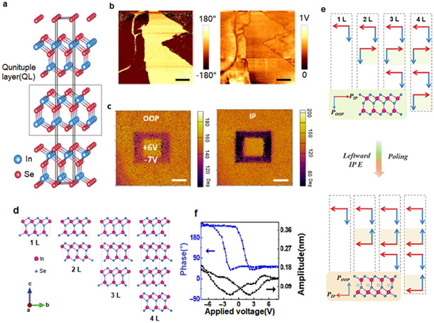
![(Color online) (a) Schematic crystal structure of In2Se3 (reproduced with permission from Ref. [77], © Ding, W. J.et al. 2017). (b) PFM phase and amplitude images of a thinα-In2Se3 flake, respectively (reproduced with permission from Ref. [45], © 2017 American Chemical Society). (c) The phase images for both OOP and IP polarization of a 6 nm thick In2Se3 flake (reproduced with permission from Ref. [46], © 2018 American Chemical Society). (d) Schematic crystal structure of 2Hα-In2Se3 in 1 to 4 layers. (e) Schematic of IP polarization rearrangement under electric field. (d) and (e) Reproduced with permission from Ref. [50], © The Royal Society of Chemistry 2021. (f) Ferroelectric hysteresis loops of 8 nm thickα-In2Se3 film (reproduced with permission from Ref. [48], © Tsinghua University Press and Springer-Verlag GmbH Germany, part of Springer Nature 2020).](/richHtml/jos/2023/44/1/011002/jos_44_1_011002_f1.jpg)
Fig. 1. (Color online) (a) Schematic crystal structure of In2Se3 (reproduced with permission from Ref. [77], © Ding, W. J.et al. 2017). (b) PFM phase and amplitude images of a thinα-In2Se3 flake, respectively (reproduced with permission from Ref. [45], © 2017 American Chemical Society). (c) The phase images for both OOP and IP polarization of a 6 nm thick In2Se3 flake (reproduced with permission from Ref. [46], © 2018 American Chemical Society). (d) Schematic crystal structure of 2Hα-In2Se3 in 1 to 4 layers. (e) Schematic of IP polarization rearrangement under electric field. (d) and (e) Reproduced with permission from Ref. [50], © The Royal Society of Chemistry 2021. (f) Ferroelectric hysteresis loops of 8 nm thickα-In2Se3 film (reproduced with permission from Ref. [48], © Tsinghua University Press and Springer-Verlag GmbH Germany, part of Springer Nature 2020).
![(Color online) (a) Schematic structure ofα-In2Se3 FeS-FET and switching characteristics ofα-In2Se3 FeS-FET (reproduced with permission from Ref. [3], Copyright © 2019, Mengwei Siet al.). (b) Schematic structure ofα-In2Se3 FeCTs and switching characteristics ofα-In2Se3 FeCTs (reproduced with permission from Ref. [19], Copyright © 2021, Shuiyuan Wanget al.).](/richHtml/jos/2023/44/1/011002/jos_44_1_011002_f2.jpg)
Fig. 2. (Color online) (a) Schematic structure ofα-In2Se3 FeS-FET and switching characteristics ofα-In2Se3 FeS-FET (reproduced with permission from Ref. [3], Copyright © 2019, Mengwei Siet al.). (b) Schematic structure ofα-In2Se3 FeCTs and switching characteristics ofα-In2Se3 FeCTs (reproduced with permission from Ref. [19], Copyright © 2021, Shuiyuan Wanget al.).
Fig. 3. (Color online) (a) Schematic crystal structure of CuInP2S6. (b) AFM images and BEPFM images of CuInP2S6 flake (reproduced with permission from Ref. [51], Copyright © 2015, American Chemical Society). (c) AFM images and PFM images of CuInP2S6 flake. (d) Electric characterization of the vdW CuInP2S6/Si diode (Inset: schematic structure of ferroelectric diode based on CuInP2S6 heterostructure). (a), (c) and (d) Reproduced with permission from Ref. [52], Copyright © 2016, Fucai Liuet al.
Fig. 4. (Color online) (a) Optical microscopy and AFM images of d1T-MoTe2. (b) PFM phase hysteretic and butterfly loops of monolayer d1T-MoTe2. (c) Schematic atomic structure of d1T-MoTe2. (d) Electric characterization and structure of the FTJ device d1T-MoTe2. (a-d) Reproduced with permission from Ref. [44], Copyright © 2019, Shuoguo Yuanet al.
Fig. 5. (Color online) (a) Schematic crystal structure of Bernal-stacked bilayer graphene (reproduced with permission from Ref. [91], © Springer Nature 2022). (b) Schematic of dual-gate devices N0, H2 and H4. (c) Four-probe resistance for devices N0, H2 and H4. (d) Hysteretic transport behavior for device H4. (Inset: ‘zigzag’ patterns illustrate how data are obtained.) (e) and (f) Forward and backward scan forVBG sweep between –50 and 50 V. (g) The difference between measured in (e) and (f). (b-g) Reproduced with permission from Ref. [74], © Zheng Zet al. 2020.
Fig. 6. (Color online) (a) Schematic crystal structure of AB-stacked and BA-stacked BN. (b) PFM phase and amplitude images of twisted bilayer BN, respectively. (c) ResistanceRxx of graphene for the device as a function of the top gate and bottom gate, respectively (Inset: dual-gate P-BBN device structure). (d) Ferroelectric switching in twisted bilayer BN. (e) Temperature dependence of polarization and graphene resistance Rxx, respectively. (f) Room-temperature operation of a ferroelectric field-effect transistor. (a-f) Reproduced with permission from Ref. [75], © 2021 American Association for the Advancement of Science.
Fig. 7. (Color online) (a) Schematic crystal structure of H-stacked and R-stacked (MX and XM) TMDs, respectively. (b) PFM phase and amplitude images of MoSe2, respectively. (c) Schematic illustration of lateral PFM measurement on MoSe2. (d) ResistanceRxx of graphene for TMDs device as a function of the top gate and bottom gate, respectively (Inset: dual-gate R-stacked TMDs device structure). (e) Ferroelectric switching in small-angel twisted bilayer WSe2 d1 device. (f) Schematic of polarization switching in WSe2 d1 and d2 device and temperature dependence of graphene resistanceRxx, respectively. (a-f) Reproduced with permission from Ref. [76], © 2021 Springer Nature 2022.
| |||||||||||||||
Table 0. Twisted 2D ferroelectricity.
| ||||||||||||
Table 0. Proved 2D ferroelectric materials.

Set citation alerts for the article
Please enter your email address


