Abstract
Since the beginning of research on two-dimensional (2D) materials, a few numbers of 2D ferroelectric materials have been predicted or experimentally confirmed, but 2D ferroelectrics as necessary functional materials are greatly important in developing future electronic devices. Recent breakthroughs in 2D ferroelectric materials are impressive, and the physical and structural properties of twisted 2D ferroelectrics, a new type of ferroelectric structure by rotating alternating monolayers to form an angle with each other, have attracted widespread interest and discussion. Here, we review the latest research on twisted 2D ferroelectrics, including Bernal-stacked bilayer graphene/BN, bilayer boron nitride, and transition metal dichalcogenides. Finally, we prospect the development of twisted 2D ferroelectrics and discuss the challenges and future of 2D ferroelectric materials.Since the beginning of research on two-dimensional (2D) materials, a few numbers of 2D ferroelectric materials have been predicted or experimentally confirmed, but 2D ferroelectrics as necessary functional materials are greatly important in developing future electronic devices. Recent breakthroughs in 2D ferroelectric materials are impressive, and the physical and structural properties of twisted 2D ferroelectrics, a new type of ferroelectric structure by rotating alternating monolayers to form an angle with each other, have attracted widespread interest and discussion. Here, we review the latest research on twisted 2D ferroelectrics, including Bernal-stacked bilayer graphene/BN, bilayer boron nitride, and transition metal dichalcogenides. Finally, we prospect the development of twisted 2D ferroelectrics and discuss the challenges and future of 2D ferroelectric materials.Introduction
Table Infomation Is Not EnableTable Infomation Is Not Enable
Ferroelectric materials, which possess spontaneous polarization that an external electric field can control, have massive potential for applications in field-effect transistors[1-13] (FETs), non-volatile memory[14-22], ferroelectric tunnel junctions (FTJ) devices[23-27], optoelectronic devices[28,29], neuromorphic computing[30-33], flexible nanoelectronics[34-36], sensors and etc.[37,38]. In 1920, ferroelectricity was first discovered by Valasek[39]. Then, ferroelectric films of perovskite structures were found in the 1950s. However, the spontaneous polarization of conventional perovskite ferroelectric thin films disappears as the film thickness is below a critical value of tens of nanometers to a few nanometers[40,41]. In the meantime, due to the rapid development of integrated circuits, the feature size of integrated devices is shrinking and the precision is increasing. The nano-scale thin ferroelectric films are becoming extremely crucial.
Since the successful exfoliation of graphene in 2004 by Novoselovet al.[42], 2D van der Waals (vdW) materials have received much attention. Compared to bulk materials, the symmetry of vdW 2D materials with weak interlayer interactions is lowered due to reduced dimensions. This opens up a new way to obtain 2D ferroelectric materials beyond the traditional limits of size and dimension[43]. 2D vdW ferroelectric materials, typically with a non-symmetry structure, can be classified into two groups, intrinsic 2D ferroelectrics and twisted 2D ferroelectrics. To date, intrinsic 2D ferroelectrics have been experimentally reported, like d1T-MoTe2[44], In2Se3[45-50], CuInP2S6[51,52], SnTe[53], WTe2[54] and BA2PbCl4[55] (Table 1). 2D vdW heterostructures can be obtained through layer-by-layer mechanical restacking, which displays unprecedented physical properties far exceeding the single layer[56]. Ferroelectric ordering arises from spontaneous symmetry breaking, and ferroelectric materials with different properties have been discovered in this system. And as the research on 2D vdW materials continued, the fabrication of heterogeneous structures became possible, and people began to realize that reducing the material size is not the only way to change the material properties, twisted 2D layered materials are also possible. The twist is a new degree of freedom that manipulate unique properties[57-73] by rotating alternating monolayers to form an angle with each other. When two layers of nonpolar materials are stacked at a certain angle, new synthetic ferroelectrics emerge, and this new way is rapidly attracting attention. It initially appeared in twisted bilayers graphene/BN[74] and then extended to other vdW layered systems, such as stacked bilayers boron nitride[75] (BN) and 2H-type transition metal dichalcogenides (TMDs)[76], MX2 (M = Mo, W; X = S, Se) (Table 2). In this review, we will divide it into four parts to illustrate intrinsic 2D ferroelectrics and summarize the current status of the twisted 2D ferroelectrics. Section 2 will briefly introduce intrinsic 2D ferroelectrics, like In2Se3, CuInP2S6 and d1T-MoTe2. In Section 3, we will review the twisted 2D ferroelectrics in detail. Finally, we will provide perspectives and conclusions on the future development of twisted 2D ferroelectrics.
Intrinsic 2D ferroelectric
Due to the rapid development of 2D layered materials with various physical properties, the realization of monolayer ferroelectric films has become possible. With the development of preparation and detection techniques, one can accurately measure the ferroelectric signal of ultrathin ferroelectrics. Intrinsic 2D ferroelectrics are a class of 2D vdW materials in which spontaneous ferroelectric polarization arises from their intrinsic structural symmetry. As a result, various 2D ferroelectric materials have been discovered. Here, we will discuss the intrinsic 2D ferroelectric materials, such as In2Se3, CuInP2S6 and d1T-MoTe2.
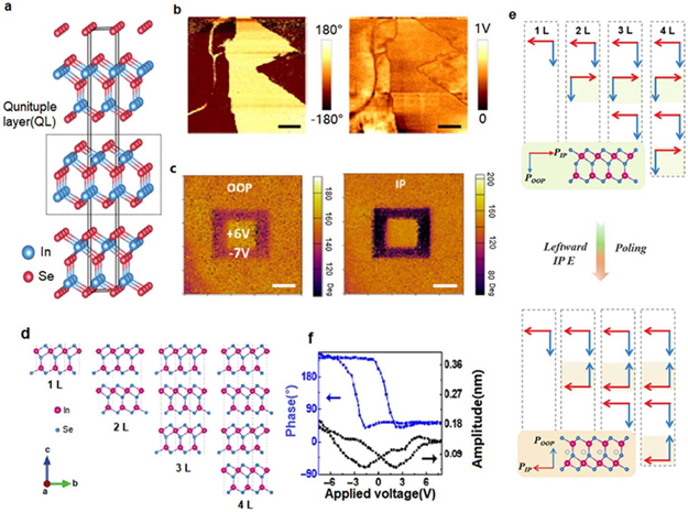
In2Se3 has five forms (α, β, γ, δ, κ) depending on the stacking order, among whichα-In2Se3 is the most stable at room temperature. In monolayer In2Se3, Se and In consist of different covalent bonds in the quintuple layer (QL) 2D In2Se3, vertically stacking by weak vdW interaction[77]. The stacking order of the five monolayers in QL is Se–In–Se–In–Se as shown inFig. 1(a). Through piezoresponse force microscopy (PFM), a 180° phase difference is observed in a 10 nm thickα-In2Se3 flake (Fig. 1(b)), corresponding to an out-of-plane (OOP) polarization that shifts from up to down perpendicular to the surface[45]. The switching ofα-In2Se3 OOP and IP polarization can be obtained by writing opposite electric field, which shows that the external electric field can control the polarization direction (Fig. 1(c)). Moreover, the IP and OOP polarizations change simultaneously, indicating that the IP polarization and OOP polarizations coexist[46]. In 2Hα-In2Se3, it possesses a special interlayer 180° IP rotation stacking structure (Fig. 1(d)) and the IP polarization directions between the layers arranged in an anti-parallel manner[50]. This indicates that the IP polarization is layer-dependent. As illustrated inFig. 1(e), for even layers, the polarizations of adjacent IP polarization directions cancel each other and the total IP polarization is zero. However, for odd layers, there is always a remnant IP polarization. When an electric field is applied in the leftward direction, the IP polarization of all layers changes its pointing to the left (Fig. 1(e)). At the same time, due to the strong intercorrelation between IP and OOP polarization, the IP and OOP polarizations are reversed at the same time, which lead to the interlayer cancellation of OOP polarizations for even layers[50]. This particular polarization relationship originates from a lateral shift of the central Se atomic layer induced by the electric field. And the local amplitude and phase shown inFig. 1(f) display a butterfly loop and hysteresis loop with a sharp phase change, which is the hallmark of ferroelectrics[48].
![(Color online) (a) Schematic crystal structure of In2Se3 (reproduced with permission from Ref. [77], © Ding, W. J.et al. 2017). (b) PFM phase and amplitude images of a thinα-In2Se3 flake, respectively (reproduced with permission from Ref. [45], © 2017 American Chemical Society). (c) The phase images for both OOP and IP polarization of a 6 nm thick In2Se3 flake (reproduced with permission from Ref. [46], © 2018 American Chemical Society). (d) Schematic crystal structure of 2Hα-In2Se3 in 1 to 4 layers. (e) Schematic of IP polarization rearrangement under electric field. (d) and (e) Reproduced with permission from Ref. [50], © The Royal Society of Chemistry 2021. (f) Ferroelectric hysteresis loops of 8 nm thickα-In2Se3 film (reproduced with permission from Ref. [48], © Tsinghua University Press and Springer-Verlag GmbH Germany, part of Springer Nature 2020).](/Images/icon/loading.gif)
Figure 1.(Color online) (a) Schematic crystal structure of In2Se3 (reproduced with permission from Ref. [77], © Ding, W. J.et al. 2017). (b) PFM phase and amplitude images of a thinα-In2Se3 flake, respectively (reproduced with permission from Ref. [45], © 2017 American Chemical Society). (c) The phase images for both OOP and IP polarization of a 6 nm thick In2Se3 flake (reproduced with permission from Ref. [46], © 2018 American Chemical Society). (d) Schematic crystal structure of 2Hα-In2Se3 in 1 to 4 layers. (e) Schematic of IP polarization rearrangement under electric field. (d) and (e) Reproduced with permission from Ref. [50], © The Royal Society of Chemistry 2021. (f) Ferroelectric hysteresis loops of 8 nm thickα-In2Se3 film (reproduced with permission from Ref. [48], © Tsinghua University Press and Springer-Verlag GmbH Germany, part of Springer Nature 2020).
The strong out-of-plane polarization ofα-In2Se3 can improve the sustainability of switchable polarization and provide a new pathway for field-effect transistors and nonvolatile memories. Based on this, Siet al.[3] proposed a novel ferroelectric semiconductor field-effect transistor (FeS-FET) as shown inFig. 2(a). The FeS-FET consists of a heavy p-type doped Si substrate as the back gate electrode, 15 nm HfO2 or 90 nm SiO2 as the gate insulating layer, 2Dα-In2Se3 as the ferroelectric semiconductor channel and 30 nm Ti/50 nm Au as the source/drain electrode. Finally, an optimized 10 nm Al2O3 capping layer is grown on top of theα-In2Se3 channel. The device exhibits high performance with a large memory window, a high switching ratio of over 108, a maximum on-state current of 862μA/μm and a low supply voltage. The conventional Fe-FET structure has a short hold time due to the depolarization field and gate leakage current[78-80]. In contrast, the FeS-FET design can eliminate the charge trap by moving charge to shield the depolarization field. At the same time, a high-quality amorphous gate insulator is chosen to eliminate the gate leakage current and improve performance. For ferroelectric memories, ferroelectric materials with two switchable stable polarization states are suitable for random access measurement systems that require easy switching between the two stable states to store information[5].α-In2Se3 exhibits strong out-of-plane ferroelectricity at room temperature and maintains ferroelectric polarization at the atomic scale, making it a basis for making nonvolatile memories. Unlike the conventional Fe-FETs, Wanget al.[19] demonstrated ferroelectric channel transistors (FeCTs) for a nonvolatile memory using the 2D ferroelectric semiconductor materialα-In2Se3 as a channel, and the structure is shown inFig. 2(b). A 30 nm Al2O3 is used as the bottom substrate layer, the conducting channel is an h-BN/α-In2Se3/h-BN layer, and a heavily p-doped Si substrate is used as the global gate (GG). With sufficient write and erase spikes, the FeCTs exhibit stable nonvolatility with high and low states exceeding 103. Meanwhile, the nonvolatility of FeCTs is programmed at a basic erase and write (LRS-HRS). The LRS-HRS ratio decreases with decreasing write width, but still writes efficiently for 40 ns, which is consistent with the ultrafast switching of ferroelectric polarization. Overall, 2Dα-In2Se3 provides a promising prospect to build high-density and high-efficiency emerging memory and computation-integrated devices as an alternative solution.
Figure 2.(Color online) (a) Schematic structure ofα-In2Se3 FeS-FET and switching characteristics ofα-In2Se3 FeS-FET (reproduced with permission from Ref. [3], Copyright © 2019, Mengwei Siet al.). (b) Schematic structure ofα-In2Se3 FeCTs and switching characteristics ofα-In2Se3 FeCTs (reproduced with permission from Ref. [19], Copyright © 2021, Shuiyuan Wanget al.).
In addition to In2Se3, CuInP2S6 and MoTe2 have also attracted extensive studies as intrinsic ferroelectrics. The atomic structure of CuInP2S6 consists of a sulfur framework in which Cu, In, and P–P triangular patterns are filled by octahedral voids. Its bulk consists of vertically stacked vdW interactions filled with weakly interacting layers (Fig. 3(a)). The ferroelectric phase transition of the bulk CuInP2S6 was first observed in 1994[81]. The origin of the ferroelectricity was demonstrated in 1997 by predicting the hopping mechanism of the thermally activated Cu(I) migration along the polar axis in the paraelectric phase[82]. About 21 years later, Belianinovet al.[51] reported that CuInP2S6 reached 50 nm experimentally, and the thickness of the films varied from 50 to 500 nm. Using band excitation PFM (BE-PFM) to detect the films, the domain with a thickness of 100 or more than 100 nm has good contrast and the 50 nm domain is likewise recognizable. However, it cannot be detected beyond this range, as inFig. 3(b). One year later, Liuet al.[52] reported the room temperature ferroelectricity of ultrathin CuInP2S6. As demonstrated inFig. 3(c), the CuInP2S6 ultrathin flakes were still ferroelectric at a thickness of a few nanometers. At the same time, a significant butterfly loop and 180° switching of the phase signal were observed at 4 nm, thus further confirming the ferroelectric polarization in ultrathin CuInP2S6. Besides, Liuet al. proposed a ferroelectric diode based on CuInP2S6/Si heterostructure using a 30 nm CuInP2S6 flake with Au as the top electrode, which can be assigned ON and OFF states, corresponding to its low and high resistance states, respectively (Fig. 3(d)).
Figure 3.(Color online) (a) Schematic crystal structure of CuInP2S6. (b) AFM images and BEPFM images of CuInP2S6 flake (reproduced with permission from Ref. [51], Copyright © 2015, American Chemical Society). (c) AFM images and PFM images of CuInP2S6 flake. (d) Electric characterization of the vdW CuInP2S6/Si diode (Inset: schematic structure of ferroelectric diode based on CuInP2S6 heterostructure). (a), (c) and (d) Reproduced with permission from Ref. [52], Copyright © 2016, Fucai Liuet al.
Compared to CuInP2S6 and In2Se3, TMDs still need to achieve ferroelectricity. Various structural phases are based on different TMD compositions, such as 2H, 1T, 1T' and d1T[83]. Among them, 2H structure is a stable semiconductor, 1T structure is unstable[84,85], and 1T' is an octahedral structure distorted from the unstable 1T structure[84,86]. And the difference between 1T' and d1T phases mainly stems from the different ways of atomic distortion. While several materials in the family of TMDs have theoretically been demonstrated to be ferroelectric potentially[87-89], few experiments have accurately confirmed their ferroelectricity. In 2019, the room-temperature ferroelectricity of monolayer d1T-MoTe2 was approved by Yuanet al.[44].Fig. 4(a) shows images of d1T-MoTe2 under optical microscopy and atomic force microscopy (AFM). d1T-MoTe2 monolayer thickness is about 0.8 nm, similar to expected. PFM measurements recorded the phase and amplitude of the out-of-plane hysteresis of monolayer d1T-MoTe2 with a 180° difference between the two polarization states, indicating room-temperature ferroelectricity. Also, the PFM phase comparison shows an antiparallel polarization of d1T-MoTe2, further confirming the d1T-MoTe2 ferroelectricity (Fig. 4(b)). To determine the intrinsic reason for the appearance of ferroelectricity in d1T-MoTe2, the structure of d1T-MoTe2 was further characterized as shown inFig. 4(c), which demonstrates the trimerized structure of d1T-MoTe2, confirming the non-centrosymmetric and similar to their calculations. Trimerized structures with vertical displacement of Te atoms cause spontaneous polarization. In addition, the monolayer d1T-MoTe2 ferroelectric film is well suited to build nanoscale nonvolatile ferroelectric tunnel junctions (FTJ) devices because of its thinnest thickness, out-of-plane polarization, and room temperature stability. In this study, a 2D vdW d1T-MoTe2/graphene FTJ device was fabricated. The two polarization directions were distinguished by representing the on and off states of the device, which has an on/off resistance ratio of about 1000 and good reproducibility (Fig. 4(d)).
Figure 4.(Color online) (a) Optical microscopy and AFM images of d1T-MoTe2. (b) PFM phase hysteretic and butterfly loops of monolayer d1T-MoTe2. (c) Schematic atomic structure of d1T-MoTe2. (d) Electric characterization and structure of the FTJ device d1T-MoTe2. (a-d) Reproduced with permission from Ref. [44], Copyright © 2019, Shuoguo Yuanet al.
In conclusion, although the current evidence is insufficient, the research has provided opportunities for potential 2D ferroelectric materials, including vdW and conventional ferroelectric materials. Based on the demand for the miniaturization of next-generation memory and logic devices, more experiments are needed to add new members to the 2D ferroelectric family. Recently a new type of stacked engineering is quietly changing the future of 2D ferroelectrics.
Twisted 2D ferroelectricity
vdW materials with natural ferroelectricity are scarce. Many layered vdW crystals, such as graphite, h-BN and TMD have a stable stacking structure and are usually centrosymmetric, so they are not qualified as ferroelectrics. However, the vertical polarization of ferroelectric materials interprets another property for the localized stacking between layers: moiré ferroelectricity. Bilayer twisted 2D ferroelectrics can induce the moiré ferroelectricity, and different ferroelectric domains can be generated by stacking. New research in stacking engineering has changed the recognition of 2D vdW ferroelectrics and brought a path to discover new ferroelectrics. In this review, we will discuss some twisted 2D ferroelectric materials including Bernal-stacked bilayer graphene/BN, bilayer boron nitride, and bilayer TMDs.
Bernal-stacked bilayer graphene/BN
Ferroelectric materials have electrically tunable electric dipoles induced by spatial separation between the average centers of positive and negative charges within a unit cell. Therefore, graphene, composed only of carbon atoms, is theoretically challenging to achieve ferroelectricity[90]. However, Zhenget al.[74] proposed a new device structure by aligning a bilayer graphene sandwiched by two BN flakes, which exhibit a significant hysteresis behavior of graphene resistance under the applied external electric field.Fig. 5(a) shows a Bernal-stacked (AB) bilayer graphene (BLG) structure with half of the carbon atoms in the upper layer on top of the empty centers of carbon hexagons in the lower layer[91].Fig. 5(b) illustrates a schematic of a bilayer graphene dual-gate device with Bernal-stack graphene sandwiched between two hexagonal boron nitrides. And there is a certain relative angle between the two BN at the top and bottle. Device H2 and H4 both use two BN flakes sandwich a BLG with different angles. The relative angles of the device H2 and H4 are 30° and 0°, respectively. H2 and H4 show striking hysteresis behavior (Fig. 5(c)). The standard BLG device N0 (without BN layers) shows no hysteresis when scanning the bottom gate voltage (VBG) or top gate voltage (VTG) backward and forward, while H2 and H4 exhibit significant hysteresis. The difference is that the resistance peak appears in the opposite sequence, showing an advanced mode for H2 and a retarded mode for H4. To explain these phenomena more closely, they tested the relationship between the four-probe resistance and the variation ofVBG andVTG.
Figure 5.(Color online) (a) Schematic crystal structure of Bernal-stacked bilayer graphene (reproduced with permission from Ref. [91], © Springer Nature 2022). (b) Schematic of dual-gate devices N0, H2 and H4. (c) Four-probe resistance for devices N0, H2 and H4. (d) Hysteretic transport behavior for device H4. (Inset: ‘zigzag’ patterns illustrate how data are obtained.) (e) and (f) Forward and backward scan forVBG sweep between –50 and 50 V. (g) The difference between measured in (e) and (f). (b-g) Reproduced with permission from Ref. [74], © Zheng Zet al. 2020.
First,VTG is in the range of –8 to 8 V,VBG is in the range of –10 to 10 V andVTG is scanning fast andVBG is scanning slow with the origin atVTG =VBG = 0 V (Fig. 5(d)). At this point, the device H4 is indistinguishable from a normal BLG. Then, reversing the scan direction and extendingVBG down to –15 V, the resistance ridge suddenly becomes parallel to theVBG axis. This behavior is like the bottom gate losing its function, which the authors describe as ‘layer-specific anomalous screening’ (LSAS). AfterVBG = –20 V, reversingVBG again (Fig. 5(d)), the LSAS phenomenon stops and restores to normal BLG behavior, however, the LSAS phenomenon also occurs after scanning a certain distance from the origin. Similarly, after reversing again, the resistance changes immediately into the normal BLG behavior, and the LSAS behavior appears after a distance beyond the origin (Figs. 5(e) and5(f)). Finally, a parallelogram formed by the resistance peaks can be obtained using the backward-and-forward scan direction (Fig. 5(g)), this points to the fact that the BLG/BN structure exhibits a dramatic hysteresis phenomenon under the action of an external electric field, demonstrating the ferroelectricity of BLG/BN. The system described in this study has strong hysteresis and stability and can be used as a high-performance memory.
The first presentation of this stacking engineering approach brings an entirely new way of thinking. It opens up a new field for vdW assembly where it is possible to create artificial vdW ferroelectric structures from non-ferroelectric material. Not only in Bernal-stacked bilayer graphene/BN, but also in bilayer twisted BN demonstrates unprecedented ferroelectricity.
Bilayer boron nitride
In 2021, Yasudaet al.[75] have revealed the electric polarization and ferroelectric switching in twisted BN with AB stacking structure. Unlike bulk hBN, bilayer BN is formed by two BN monolayers stacked in parallel with two polarization AB or BA stacking orders[92,93]. In the AB (BA) stack, the B (N) atoms in the upper layer are on top of the N (B) atom in the lower layer while the N (B) atom in the upper layer is on top of the B (N) lower in an atom (Fig. 6(a)). Using PFM, the polarization of small-angle twisted bilayer BN have been probed, where the different piezoelectric response of AB and BA domain regions responds to different out-of-plane polarization (Fig. 6(b))[94]. Interestingly, the out-of-plane polarization is correlated with the stacking order. Namely, the polarization can be switched by the shear motion of one-third of a unit cell[94], which differs from the conventional ferroelectric switching mechanism. Yasudaet al. fabricated a dual-gate device composed by metal top gate (Au/Cr)/hBN/Graphene/bilayer 0° parallel stacked BN (P-BBN)/hBN/metal bottom gate (PdAu).Fig. 6(c) demonstrates the graphene resistance as a function of top gate voltage (VT), by scanning the top gate backward and forward, and no hysteresis phenomenon is observed. In contrast, a clear hysteresis phenomenon can be seen (Fig. 6(c)) as the bottom gate is scanned backward and forward to explore the graphene resistance related to the bottom gate voltage (VB). For a dual-gate scan can independently control the charge on graphene and the electric field on P-BBN, the standard dual-gate device have a unique diagonal resistance peak characteristic, which corresponds to the charge neutralization condition, following the equation:
, where
is the charge permittivity of hBN,
and
are the distances from the bottom gate electrode and the top gate electrode to the graphene, respectively, and
is the charge. As illustrated inFig. 6(d), the device T1 which composed by metal top gate (Au/Cr)/hBN/Graphene/bilayer 0.6° parallel stacked BN (P-BBN)/hBN/metal bottom gate (PdAu) exhibit two diagonal peaks, corresponding to BA and AB stacking, respectively. Instead of abrupt changes, the two diagonals gradually shift to the other diagonal, the origin is mainly due to the change of domains from the BA stack to the AB stack (shown in the inset). As the polarization flips, the total carrier concentration changes from
(BA stack) to
(AB stack), resulting in a shift of the resistive peak. Comparing the twisted and non-twisted devices, there are two differences: (1) The coercive field of the twisted bilayer BN is much smaller than that of the non-twisted bilayer BN. (2) The polarization switching of the twisted bilayer BN occurs slowly, and the polarization switching of the non-twisted bilayer BN changes sharply. Finally, the temperature and polarization relationship of P-BBN is demonstrated inFig. 6(e). Remarkably, the measured polarization is almost independent of temperature below room temperature[92]. The thermal vibration of atoms within in-plane is inhibited by the covalent bonds within the intralayer, making the polarization insensitive to temperature. Although an increasing temperature causes a broadening of the resistance peak, the ferroelectric hysteresis phenomenon is still persisted at room temperature. Such a feature allows a bilayer BN to write polarization by a voltage pulse of a few Volts and read it in a nonvolatile way (Fig. 6(f)). These works’ research expands the prospects of 2D ferroelectric materials for electronic, spintronic and optical applications.
Figure 6.(Color online) (a) Schematic crystal structure of AB-stacked and BA-stacked BN. (b) PFM phase and amplitude images of twisted bilayer BN, respectively. (c) ResistanceRxx of graphene for the device as a function of the top gate and bottom gate, respectively (Inset: dual-gate P-BBN device structure). (d) Ferroelectric switching in twisted bilayer BN. (e) Temperature dependence of polarization and graphene resistance Rxx, respectively. (f) Room-temperature operation of a ferroelectric field-effect transistor. (a-f) Reproduced with permission from Ref. [75], © 2021 American Association for the Advancement of Science.
Transition metal dichalcogenides (TMDs)
Similarly, synthetic ferroelectricity was achieved in the twisted TMDs system. In the conventional 2D ferroelectrics, the ferroelectricity of 1T phase TMDs have been predicted or experimentally confirmed[90]. The bulk TMD crystal is the symmetric inversion, but the symmetry is broken when exfoliated to a monolayer. Alternatively, the symmetry of TMDs can be tuned by controlling the stacking angle of two monolayers. When two layers are stacked in an antiparallel manner, the hexagonal-stacked (H-stacked) is formed and symmetry is restored. Conversely, when two layers are stacked in parallel, the rhombohedral-stacked (R-stacked) is formed[95], which breaks the out-of-plane mirror symmetry. There are two forms of R-stacked arrangements, MX- and XM-stacked forms. In MX-stacked, every M-atom is on top of an X-atom, and in XM-stacked, each X-atom is located on an M-atom[96] (Fig. 7(a)). At the same time, the two stacking orders are converted by lateral shift. The out-of-plane polarization is switched to each other by interlayer shear motion, thus achieving interfacial ferroelectricity[94]. Wanget al.[76] has revealed ferroelectricity in twisted MoS2, MoSe2, WS2 and WSe2.Fig. 7(b) shows the PFM image of 0.25° bilayer twisted MoSe2 at room-temperature, showing clear contrast between MX and XM domains with opposite out-of-plane polarization for each adjacent domain, originating from the piezoelectric or electrostatic effects[96]. Lateral PFM images of 0.2° bilayer twisted MoSe2 inFig. 7(c) are applied to study the response of the opposite out-of-plane polarization of MX and XM domains under out-of-plane electric fields. As the bottom voltageVB changes from –4 to 2 V, the domain walls move, causing the domains to shrink until it disappears, and whenVB is swept back, the domains expand. Furthermore, Wanget al. fabricated a dual-gate device comprising R-stacked bilayer twisted TMDs as shown in the inset ofFig. 7(d), which demonstrates the ferroelectricity by recording the graphene resistance as a function of the bottom gate. The structure of both device d1 and d2 from top to bottom are the metal Au/Cr, top hBN flake, 0° bilayer WSe2, bottom hBN flake and graphene, while the top hBN thickness (dT) of d1 device is 25.6 nm and thedT of d2 device is 16.1 nm.Fig. 7(d) displays the twisted bilayer WSe2, MoSe2, WS2, and MoS2 devices, respectively. They all show prominent hysteresis when sweeping the bottom gate, and the hysteresis mainly originates from the change of MX (XM)-stacked to XM (MX)-stacked. The hysteresis only occurs as the bottom gate scan indicates that the hysteresis originates from the bilayer twisted TMDs between the bottom gate and graphene. Further, ferroelectric polarization changes the carrier concentration in graphene, causing a shift of graphene resistance peak. Thus, the 0° bilayer WSe2 d1 device exhibits a diagonal feature corresponding to the graphene charge neutrality point resistance peak for a fast scan of the top gate and a slow scan of the bottom gate. As the bottom gate is swept backward, the diagonal feature of the graphene resistance peak changes abruptly (Fig. 7(e)). The shift of the resistance peak is due to the carrier concentration change caused by the electric polarization of the R-stacked bilayer twisted TMDs, which, like the bilayer twisted BN, changes from
(Up polarization) to
(Down polarization). Unlike the 0° bilayer WSe2 d1 device, the 0° bilayer WSe2 d2 device (dT is 16.1 nm) has a stepped ferroelectric polarization switching (Fig. 7(f)). The independent shift of every domain wall causes this multi-step switching. InFig. 7(g), the 0° bilayer WSe2 d1 device can maintain ferroelectricity at room temperature. The R-stacked bilayer TMDs can embed ferroelectricity in the semiconductor to realize ferroelectric semiconductor field-effect transistors[97].
Figure 7.(Color online) (a) Schematic crystal structure of H-stacked and R-stacked (MX and XM) TMDs, respectively. (b) PFM phase and amplitude images of MoSe2, respectively. (c) Schematic illustration of lateral PFM measurement on MoSe2. (d) ResistanceRxx of graphene for TMDs device as a function of the top gate and bottom gate, respectively (Inset: dual-gate R-stacked TMDs device structure). (e) Ferroelectric switching in small-angel twisted bilayer WSe2 d1 device. (f) Schematic of polarization switching in WSe2 d1 and d2 device and temperature dependence of graphene resistanceRxx, respectively. (a-f) Reproduced with permission from Ref. [76], © 2021 Springer Nature 2022.
Stacking engineering opens new directions for the discovery of ferroelectric materials. Theoretically, any two nonpolar vdW layered structures can be stacked together to achieve ferroelectricity heterogeneous/homogeneous structures as long as the inversion symmetry is broken at the interface. Such an approach dramatically expands the variety of 2D vdW ferroelectric materials. In the future, it may involve coupling between different types of materials, giving rise to the discovery of more novel materials, such as coupling with magnetic vdW materials, which may lead to the discovery of atomically thin multiferroic vdW systems. Although twisted 2D ferroelectrics have fantastic potential, people need more time to explore various physical mechanisms due to stacking and face many challenges, such as stability, scalability, and practical applications in electronic devices. Our discussion here is just the beginning of this new field.
Summary and perspective
The twisted 2D ferroelectrics based on stacking-engineered is a new and promising research field. It has many unknown phenomena and essences. In this review, we summarize the recent research and progress of twisted 2D ferroelectrics and provide a platform for subsequent practical and theoretical studies. Traditional 3D ferroelectric materials have been successfully used in many industrial applications, driving the rapid development of technology. With the development of characterization and fabrication methods, there will be more and more ways to discover new twisted 2D ferroelectric materials and reveal their unique physical properties and mechanisms.
Generally, this stacking-engineered design approach for twisted 2D ferroelectrics can be extended to other 2D vdW materials, such as group III chalcogenides GaS, GaSe and InSe[94], and even 2D ferromagnetic insulator CrI3, to explore novel twisted 2D multiferroics. Meanwhile, the distinctive physical properties of twisted 2D ferroelectric materials empower next-generation electronic devices with high performance, low power consumption and high integration, for example, non-volatile memory with a high switching ratio and low leakage current, new Fe-FET and the ability to complete the neural network calculation of the memory and computing integrated device has great potential. Still, at present, the design of electronic devices using twisted 2D ferroelectrics is very lacking, the main reason is that for the new type of ferroelectrics, people still need to be more explicit about its internal mechanisms. This is something that needs to be gradually explored in future research. At present, only a few vdW materials can maintain ferroelectricity for a long time at room temperature. There is an urgent need to develop new approaches to improve their stability, as well as twisted 2D ferroelectrics are currently insufficient in optical, electrical, thermal, mechanical and magnetic studies, and probing tiny ferroelectric polarization is still a significant challenge. Finally, the ultimate goal of 2D ferroelectric materials is to design intelligent devices with better performance, so more 2D ferroelectric materials with ideal properties and new corresponding intelligent device structures need to be discovered and realized. In summary, the study of twisted 2D vdW ferroelectrics is still in its infancy. It requires further exploration not only in the material selection but also in the potential mechanisms and properties. And this research may lead to exciting breakthroughs in nanoelectronics, photonics, non-volatile memory, memory and computation integration and communication.
Acknowledgements
We acknowledge the financial support from National Science Foundation of China (51872039, 52021001, 5197204).
References
[1] X J Chai, J Jiang, Q H Zhang et al. Nonvolatile ferroelectric field-effect transistors. Nat Commun, 11, 2811(2020).
[2] R C G Naber, C Tanase, P W M Blom et al. High-performance solution-processed polymer ferroelectric field-effect transistors. Nature Mater, 4, 243(2005).
[3] M W Si, A K Saha, S J Gao et al. A ferroelectric semiconductor field-effect transistor. Nat Electron, 2, 580(2019).
[4] M W Si, P Y Liao, G Qiu et al. Ferroelectric field-effect transistors based on MoS2 and CuInP2S6 two-dimensional van der waals heterostructure. ACS Nano, 12, 6700(2018).
[5] S Y Wan, Y Li, W Li et al. Nonvolatile ferroelectric memory effect in ultrathin α-In2Se3. Adv Funct Mater, 29, 1808606(2019).
[6] Z D Luo, M M Yang, Y Liu et al. Emerging opportunities for 2D semiconductor/ferroelectric transistor-structure devices. Adv Mater, 33, 2005620(2021).
[7] G Wu, B Tian, L Liu et al. Programmable transition metal dichalcogenide homojunctions controlled by nonvolatile ferroelectric domains. Nat Electron, 3, 43(2020).
[8] Z D Luo, X Xia, M M Yang et al. Artificial optoelectronic synapses based on ferroelectric field-effect enabled 2D transition metal dichalcogenide memristive transistors. ACS Nano, 14, 746(2020).
[9] L Lv, F W Zhuge, F J Xie et al. Reconfigurable two-dimensional optoelectronic devices enabled by local ferroelectric polarization. Nat Commun, 10, 3331(2019).
[10] T Li, P Sharma, A Lipatov et al. Polarization-mediated modulation of electronic and transport properties of hybrid MoS2-BaTiO3-SrRuO3 tunnel junctions. Nano Lett, 17, 922(2017).
[11] X Wang, P Wang, J Wang et al. Ultrasensitive and broadband MoS2 photodetector driven by ferroelectrics. Adv Mater, 27, 6575(2015).
[12] A Lipatov, P Sharma, A Gruverman et al. Optoelectrical molybdenum disulfide (MoS2)—Ferroelectric memories. ACS Nano, 9, 8089(2015).
[13] H S Lee, S W Min, M K Park et al. MoS2Nanosheets for top-gate nonvolatile memory transistor channel. Small, 8, 3111(2012).
[14] J F Scott, C A Paz de Araujo. Ferroelectric memories. Science, 246, 1400(1989).
[15] A Q Jiang, C Wang, K J Jin et al. A resistive memory in semiconducting BiFeO3 thin-film capacitors. Adv Mater, 23, 1277(2011).
[16] H Ishiwara. Ferroelectric random access memories. J Nanosci Nanotechnol, 12, 7619(2012).
[17] T Mikolajick, S Slesazeck, M H Park et al. Ferroelectric hafnium oxide for ferroelectric random-access memories and ferroelectric field-effect transistors. MRS Bull, 43, 340(2018).
[18] S D Hyun, H W Park, M H Park et al. Field-induced ferroelectric Hf1–xZrxO2 thin films for high-k dynamic random access memory. Adv Electron Mater, 6, 2000631(2020).
[19] S Wang, L Liu, L Gan et al. Two-dimensional ferroelectric channel transistors integrating ultra-fast memory and neural computing. Nat Commun, 12, 1(2021).
[20] M Dai, K Li, F Wang et al. Intrinsic dipole coupling in 2D van der Waals ferroelectrics for gate-controlled switchable rectifier. Adv Electron Mater, 6, 1900975(2020).
[21] S Y Wan, Y Li, W Li et al. Room-temperature ferroelectricity and a switchable diode effect in two-dimensional α-In2Se3 thin layers. Nanoscale, 10, 14885(2018).
[22] S M Poh, S J R Tan, H Wang et al. Molecular-beam epitaxy of two-dimensional In2Se3 and its giant electroresistance switching in ferroresistive memory junction. Nano Lett, 18, 6340(2018).
[23] J Yoon, S Hong, Y W Song et al. Understanding tunneling electroresistance effect through potential profile in Pt/Hf0.5Zr0.5O2/TiN ferroelectric tunnel junction memory. Appl Phys Lett, 115, 153502(2019).
[24] Y Goh, S Jeon. Enhanced tunneling electroresistance effects in HfZrO-based ferroelectric tunnel junctions by high-pressure nitrogen annealing. Appl Phys Lett, 113, 052905(2018).
[25] F Ambriz-Vargas, G Kolhatkar, M Broyer et al. A complementary metal oxide semiconductor process-compatible ferroelectric tunnel junction. ACS Appl Mater Interfaces, 9, 13262(2017).
[26] J Y Park, K Yang, D H Lee et al. A perspective on semiconductor devices based on fluorite-structured ferroelectrics from the materials–device integration perspective. J Appl Phys, 128, 240904(2020).
[27] Z Xi, J Ruan, C Li et al. Giant tunnelling electroresistance in metal/ferroelectric/semiconductor tunnel junctions by engineering the Schottky barrier. Nat Commun, 8, 1(2017).
[28] F Xue, X He, W Liu et al. Optoelectronic ferroelectric domain‐wall memories made from a single Van Der Waals ferroelectric. Adv Funct Mater, 30, 2004206(2020).
[29] K Xu, W Jiang, X S Gao et al. Optical control of ferroelectric switching and multifunctional devices based on van der Waals ferroelectric semiconductors. Nanoscale, 12, 23488(2020).
[30] L Wang, X Wang, Y Zhang et al. Exploring ferroelectric switching in α-In2Se3 for neuromorphic computing. Adv Funct Mater, 30, 2004609(2020).
[31] Y S Zhang, L Wang, H Chen et al. Analog and digital mode α-In2Se3 memristive devices for neuromorphic and memory applications. Adv Electron Mater, 7, 2100609(2021).
[32] K C Kwon, Y S Zhang, L Wang et al. In-plane ferroelectric tin monosulfide and its application in a ferroelectric analog synaptic device. ACS Nano, 14, 7628(2020).
[33] J H Bian, Z Y Cao, P Zhou. Neuromorphic computing: Devices, hardware, and system application facilitated by two-dimensional materials. Appl Phys Rev, 8, 041313(2021).
[34] M Dai, Z Wang, F Wang et al. Two-dimensional van der Waals materials with aligned in-plane polarization and large piezoelectric effect for self-powered piezoelectric sensors. Nano Lett, 19, 5410(2019).
[35] H J Kim, K Schanze. Introducing ACS applied electronic materials. ACS Appl Electron Mater, 1, 1(2019).
[36] F Xue, J Zhang, W Hu et al. Multidirection piezoelectricity in mono- and multilayered hexagonal α-In2Se3. ACS Nano, 12, 4976(2018).
[37] J F Scott. Applications of modern ferroelectrics. Science, 315, 954(2007).
[38] V K Prateek, R K Thakur. Recent progress on ferroelectric polymer-based nanocomposites for high energy density capacitors: Synthesis, dielectric properties, and future aspects. Chem Rev, 116, 4260(2016).
[39] J Valasek. Piezo-electric and allied phenomena in rochelle salt. Phys Rev, 17, 475(1921).
[40] J Junquera, P Ghosez. Critical thickness for ferroelectricity in perovskite ultrathin films. Nature, 422, 506(2003).
[41] D D Fong, G B Stephenson, S K Streiffer et al. Ferroelectricity in ultrathin perovskite films. Science, 304, 1650(2004).
[42] K S Novoselov, A K Geim, S V Morozov et al. Electric field effect in atomically thin carbon films. Science, 306, 666(2004).
[43] D Lee, H Lu, Y Gu et al. Emergence of room-temperature ferroelectricity at reduced dimensions. Science, 349, 1314(2015).
[44] S G Yuan, X Luo, H L Chan et al. Room-temperature ferroelectricity in MoTe2 down to the atomic monolayer limit. Nat Commun, 10, 1775(2019).
[45] Y Zhou, D Wu, Y H Zhu et al. Out-of-plane piezoelectricity and ferroelectricity in layered α-In2Se3 nanoflakes. Nano Lett, 17, 5508(2017).
[46] C Cui, W J Hu, X Yan et al. Intercorrelated in-plane and out-of-plane ferroelectricity in ultrathin two-dimensional layered semiconductor In2Se3. Nano Lett, 18, 1253(2018).
[47] J Xiao, H Zhu, Y Wang et al. Intrinsic two-dimensional ferroelectricity with dipole locking. Phys Rev Lett, 120, 227601(2018).
[48] W F Io, S G Yuan, S Y Pang et al. Temperature- and thickness-dependence of robust out-of-plane ferroelectricity in CVD grown ultrathin van der Waals α-In2Se3 layers. Nano Res, 13, 1897(2020).
[49] C Zheng, L Yu, L Zhu et al. Room temperature in-plane ferroelectricity in van der Waals In2Se3. Sci Adv, 4, eaar7720(2018).
[50] B Lv, Z Yan, W Xue et al. Layer-dependent ferroelectricity in 2H-stacked few-layer α-In2Se3. Mater Horiz, 8, 1472(2021).
[51] A Belianinov, Q He, A Dziaugys et al. CuInP2S6 room temperature layered ferroelectric. Nano Lett, 15, 3808(2015).
[52] F C Liu, L You, K L Seyler et al. Room-temperature ferroelectricity in CuInP2S6 ultrathin flakes. Nat Commun, 7, 12357(2016).
[53] K Chang, J Liu, H Lin et al. Discovery of robust in-plane ferroelectricity in atomic-thick SnTe. Science, 353, 274(2016).
[54] Z Fei, W Zhao, T A Palomaki et al. Ferroelectric switching of a two-dimensional metal. Nature, 560, 336(2018).
[55] L You, F C Liu, H S Li et al. In-plane ferroelectricity in thin flakes of van der waals hybrid perovskite. Adv Mater, 30, 1803249(2018).
[56] A K Geim, I V Grigorieva. Van der Waals heterostructures. Nature, 499, 419(2013).
[57] Morell E Suárez, J D Correa, P Vargas et al. Flat bands in slightly twisted bilayer graphene: Tight-binding calculations. Phys Rev B, 82, 121407(2010).
[58] M Yankowitz, S Chen, H Polshyn et al. Tuning superconductivity in twisted bilayer graphene. Science, 363, 1059(2019).
[59] L Wang, E M Shih, A Ghiotto et al. Correlated electronic phases in twisted bilayer transition metal dichalcogenides. Nat Mater, 19, 861(2020).
[60] Y H Tang, L Z Li, T X Li et al. Simulation of Hubbard model physics in WSe2/WS2 moiré superlattices. Nature, 579, 353(2020).
[61] C Shen, Y Chu, Q Wu et al. Correlated states in twisted double bilayer graphene. Nat Phys, 16, 520(2020).
[62] A L Sharpe, E J Fox, A W Barnard et al. Emergent ferromagnetism near three-quarters filling in twisted bilayer graphene. Science, 365, 605(2019).
[63] M Serlin, C L Tschirhart, H Polshyn et al. Intrinsic quantized anomalous Hall effect in a moiré heterostructure. Science, 367, 900(2020).
[64] E C Regan, D Wang, C Jin et al. Mott and generalized Wigner crystal states in WSe2/WS2 moiré superlattices. Nature, 579, 359(2020).
[65] X Liu, Z Hao, E Khalaf et al. Tunable spin-polarized correlated states in twisted double bilayer graphene. Nature, 583, 221(2020).
[66] G H Li, A Luican, J M B Lopes dos Santos et al. Observation of Van Hove singularities in twisted graphene layers. Nat Phys, 6, 109(2010).
[67] G R Chen, A L Sharpe, E J Fox et al. Tunable correlated Chern insulator and ferromagnetism in a moiré superlattice. Nature, 579, 56(2020).
[68] G R Chen, L L Jiang, S Wu et al. Evidence of a gate-tunable Mott insulator in a trilayer graphene moiré superlattice. Nat Phys, 15, 237(2019).
[69] Y Cao, D Rodan-Legrain, O Rubies-Bigorda et al. Tunable correlated states and spin-polarized phases in twisted bilayer-bilayer graphene. Nature, 583, 215(2020).
[70] Y Cao, V Fatemi, S A Fang et al. Unconventional superconductivity in magic-angle graphene superlattices. Nature, 556, 43(2018).
[71] Y Cao, V Fatemi, A Demir et al. Correlated insulator behaviour at half-filling in magic-angle graphene superlattices. Nature, 556, 80(2018).
[72] G W Burg, J H Zhu, T Taniguchi et al. Correlated insulating states in twisted double bilayer graphene. Phys Rev Lett, 123, 197702(2019).
[73] R Bistritzer, A H MacDonald. Moiré bands in twisted double-layer graphene. PNAS, 108, 12233(2011).
[74] Z R Zheng, Q Ma, Z Bi et al. Unconventional ferroelectricity in moiré heterostructures. Nature, 588, 71(2020).
[75] K Yasuda, X Wang, K Watanabe et al. Stacking-engineered ferroelectricity in bilayer boron nitride. Science, 372, 1458(2021).
[76] X Wang, K Yasuda, Y Zhang et al. Interfacial ferroelectricity in rhombohedral-stacked bilayer transition metal dichalcogenides. Nat Nanotechnol, 17, 367(2022).
[77] W J Ding, J B Zhu, Z Wang et al. Prediction of intrinsic two-dimensional ferroelectrics in In2Se3 and other III2-VI3 van der Waals materials. Nat Commun, 8, 14956(2017).
[78] H Ishiwara. Current status and prospects of FET-type ferroelectric memories. International Electron Devices Meeting, 1, 725(2001).
[79] T P Ma, J P Han. Why is nonvolatile ferroelectric memory field-effect transistor still elusive. IEEE Electron Device Lett, 23, 386(2002).
[80] E Yurchuk, J Muller, S Muller et al. Charge-trapping phenomena in HfO2-based FeFET-type nonvolatile memories. IEEE Trans Electron Devices, 63, 3501(2016).
[81] A Simon, J Ravez, V Maisonneuve et al. Paraelectric-ferroelectric transition in the lamellar thiophosphate CuInP2S6. Chem Mater, 6, 1575(1994).
[82] V Maisonneuve, J M Reau, M Dong et al. Ionic conductivity in ferroic CuInP2S6 and CuCrP2S6. Ferroelectrics, 196, 257(1997).
[83] H J Kim, S H Kang, I Hamada et al. Origins of the structural phase transitions in MoTe2 and WTe2. Phys Rev B, 95, 180101(2017).
[84] D H Keum, S Cho, J H Kim et al. Bandgap opening in few-layered monoclinic MoTe2. Nat Phys, 11, 482(2015).
[85] X F Qian, J W Liu, L Fu et al. Quantum spin Hall effect in two-dimensional transition metal dichalcogenides. Science, 346, 1344(2014).
[86] G Eda, T Fujita, H Yamaguchi et al. Coherent atomic and electronic heterostructures of single-layer MoS2. ACS Nano, 6, 7311(2012).
[87] E Bruyer, D Di Sante, P Barone et al. Possibility of combining ferroelectricity and Rashba-like spin splitting in monolayers of the 1 T-type transition-metal dichalcogenides MX2 (M = Mo, W; X = S, Se, Te). Phys Rev B, 94, 195402(2016).
[88] S N Shirodkar, U V Waghmare. Emergence of ferroelectricity at a metal-semiconductor transition in a 1T monolayer of MoS2. Phys Rev Lett, 112, 157601(2014).
[89] Q Yang, M H Wu, J Li. Origin of two-dimensional vertical ferroelectricity in WTe2 bilayer and multilayer. J Phys Chem Lett, 9, 7160(2018).
[90] A H Castro Neto, F Guinea, N M R Peres et al. The electronic properties of graphene. Rev Mod Phys, 81, 109(2009).
[91] S C de la Barrera, S Aronson, Z R Zheng et al. Cascade of isospin phase transitions in Bernal-stacked bilayer graphene at zero magnetic field. Nat Phys, 18, 771(2022).
[92] G Constantinescu, A Kuc, T Heine. Stacking in bulk and bilayer hexagonal boron nitride. Phys Rev Lett, 111, 036104(2013).
[93] H J Park, J Cha, M Choi et al. One-dimensional hexagonal boron nitride conducting channel. Sci Adv, 6, eaay4958(2020).
[94] L Li, M H Wu. Binary compound bilayer and multilayer with vertical polarizations: Two-dimensional ferroelectrics, multiferroics, and nanogenerators. ACS Nano, 11, 6382(2017).
[95] L C Towle, V Oberbeck, B E Brown et al. Molybdenum diselenide: Rhombohedral high pressure-high temperature polymorph. Science, 154, 895(1966).
[96] A Weston, Y Zou, V Enaldiev et al. Atomic reconstruction in twisted bilayers of transition metal dichalcogenides. Nat Nanotechnol, 15, 592(2020).
[97] C J Cui, F Xue, W J Hu et al. Two-dimensional materials with piezoelectric and ferroelectric functionalities. npj 2D Mater Appl, 2, 18(2018).