• Journal of Infrared and Millimeter Waves
  • Vol. 40, Issue 6, 709 (2021)
Wen-Cheng YUE1、*, Qing WANG1、2, Xin-Yu LI1、3, Shu-Xiao WANG1、2, and Ming-Bin YU1、4
Author Affiliations
  • 1Laboratory of Silicon-Based Materials and Integrated Devices,Shanghai Institute of Microsystem and Information Technology,Chinese Academy of Sciences,Shanghai 200050,China
  • 2University of Chinese Academy of Sciences,Beijing 100049,China
  • 3Department of Electronic Engineering,Xi’an University of Technology,Xi’an 710048,China
  • 4Shanghai Industrial μTechnology Research Institute,Shanghai 201800,China
  • show less
    DOI: 10.11972/j.issn.1001-9014.2021.06.001 Cite this Article
    Wen-Cheng YUE, Qing WANG, Xin-Yu LI, Shu-Xiao WANG, Ming-Bin YU. All-dielectric antislot waveguide with subwavelength mode confinement and its high-efficiency coupling with input/output fiber[J]. Journal of Infrared and Millimeter Waves, 2021, 40(6): 709 Copy Citation Text show less
    (a)Three-dimensional structural diagram of the all-dielectric antislot waveguide,(b)its cross-section,(c)partial enlarged view of (b)Note:(a),(b),and (c)are all not drawn to scale
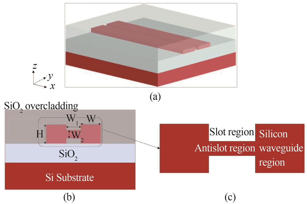
    Fig. 1. (a)Three-dimensional structural diagram of the all-dielectric antislot waveguide,(b)its cross-section,(c)partial enlarged view of (b)Note:(a),(b),and (c)are all not drawn to scale
    (a)Influence of structural parameters on normalized mode area of the all-dielectric antislot waveguide,(b)normalized electromagnetic energy density and electric vector distributions at W = 150 nm,W1 = 50 nm,and W2 = 20 nm. The definition of W,W1,and W2 is shown in Fig. 1(b)Note:The height of the waveguide is 220 nm
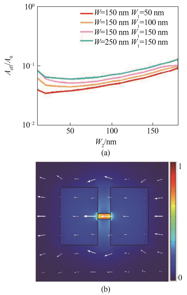
    Fig. 2. (a)Influence of structural parameters on normalized mode area of the all-dielectric antislot waveguide,(b)normalized electromagnetic energy density and electric vector distributions at W = 150 nm,W1 = 50 nm,and W2 = 20 nm. The definition of WW1,and W2 is shown in Fig. 1(b)Note:The height of the waveguide is 220 nm
    (a)The light coupling structure from the lensed fiber to the antislot waveguide or vice versa,(b)partial enlarged view of (a)Note:(a)and (b)are both not drawn to scale. The zero in y and z directions is located at the middle of the coupling structure and the middle of the top silicon,respectively
    Fig. 3. (a)The light coupling structure from the lensed fiber to the antislot waveguide or vice versa,(b)partial enlarged view of (a)Note:(a)and (b)are both not drawn to scale. The zero in y and z directions is located at the middle of the coupling structure and the middle of the top silicon,respectively
    Influence of the lensed fiber position on coupling efficiency and loss in (a)z and (b)y directions. The optimal fiber position in z and y directions is approximately located at 1.4 μm and 0,respectively
    Fig. 4. Influence of the lensed fiber position on coupling efficiency and loss in (a)z and (b)y directions. The optimal fiber position in z and y directions is approximately located at 1.4 μm and 0,respectively
    Coupling efficiency (a)from the lensed fiber to the silicon waveguide as a function of the inverse taper length (L1)with the lensed fiber at the optimal position and (b)from the silicon waveguide to the antislot waveguide as a function of the adiabatic linear taper length (L2)
    Fig. 5. Coupling efficiency (a)from the lensed fiber to the silicon waveguide as a function of the inverse taper length (L1)with the lensed fiber at the optimal position and (b)from the silicon waveguide to the antislot waveguide as a function of the adiabatic linear taper length (L2
    Electromagnetic energy transfer process from the silicon waveguide to the antislot waveguide (a),(c)at the xz section with y = 0,(b),(d)at the xy section with z = 0 Note:(a)and (b)correspond to the case when the length of the adiabatic linear taper is 8 μm,(c)and (d)are the case of without the adiabatic linear taper
    Fig. 6. Electromagnetic energy transfer process from the silicon waveguide to the antislot waveguide (a),(c)at the xz section with y = 0,(b),(d)at the xy section with z = 0 Note:(a)and (b)correspond to the case when the length of the adiabatic linear taper is 8 μm,(c)and (d)are the case of without the adiabatic linear taper
    Electromagnetic energy transfer process from the antislot waveguide to the output end (a)the length of the antislot waveguide,the adiabatic linear taper,the silicon waveguide and the inverse taper is 4 μm,8 μm,2 μm and 10 μm,respectively,(b)corresponds to the case of without the adiabatic linear taper
    Fig. 7. Electromagnetic energy transfer process from the antislot waveguide to the output end (a)the length of the antislot waveguide,the adiabatic linear taper,the silicon waveguide and the inverse taper is 4 μm,8 μm,2 μm and 10 μm,respectively,(b)corresponds to the case of without the adiabatic linear taper
    Wen-Cheng YUE, Qing WANG, Xin-Yu LI, Shu-Xiao WANG, Ming-Bin YU. All-dielectric antislot waveguide with subwavelength mode confinement and its high-efficiency coupling with input/output fiber[J]. Journal of Infrared and Millimeter Waves, 2021, 40(6): 709
    Download Citation