1Laboratory of Silicon-Based Materials and Integrated Devices,Shanghai Institute of Microsystem and Information Technology,Chinese Academy of Sciences,Shanghai 200050,China
2University of Chinese Academy of Sciences,Beijing 100049,China
3Department of Electronic Engineering,Xi’an University of Technology,Xi’an 710048,China
4Shanghai Industrial μTechnology Research Institute,Shanghai 201800,China
Due to metallic ohmic loss, plasmonic waveguides usually have larger propagation loss. Here, an all-dielectric antislot waveguide was proposed, which can realize subwavelength mode confinement and theoretically lossless propagation simultaneously. A normalized mode area of 3.4×10⁻² was achieved in the all-dielectric antislot waveguide. Moreover, an efficient coupling scheme between the small-size antislot waveguide and input/output fiber was proposed. An overall coupling efficiency of 92.7% was attained. The misalignment tolerance for 1 dB loss penalty was about 2 μm in both y and z directions.
In the highly informational age,it has become an inevitable trend to reduce the physical size of devices down to subwavelength scale to satisfy the growing demand for lower power consumption and higher data bandwidth of photonic devices[1-2]. Confining light in subwavelength scale can greatly enhance the light-matter interactions[3-11],which can be used to realize ultra-compact low-threshold lasers[6,12-14],nonlinear enhancement[15-16],high-efficient solar cells[17-20],high-speed optical signal processing[21-24],high-sensitivity sensors[25-27],and so on. In recent years,in the realization of strong optical mode confinement,surface plasmon polaritons (SPPs)[28-30] have gotten extensive attention. Photonic devices based on SPPs can break through the diffraction limit of light and allow for photonic integration with subwavelength mode confinement. However,stronger mode confinement of plasmonic waveguides is always accompanied by higher propagation loss. The trade-off between mode confinement and propagation loss is a typical challenge in plasmonic waveguides. The slot waveguide proposed by M. Lipson’s group can guide and confine light in nanometer-size low-refractive-index material[31-32]. However,the confinement is limited only in the direction perpendicular to the slot. In this article,an all-dielectric antislot waveguide was proposed in order to realize subwavelength mode confinement in the plane perpendicular to the direction of wave propagation. Because of excluding metal materials,all-dielectric waveguide has a natural advantage over its plasmonic counterparts in terms of propagation loss. Actually,subwavelength mode confinement and lossless propagation in theory can be achieved synchronously in the proposed antislot waveguide,conquering the trade-off between the two physical quantities. We also proposed an efficient scheme to improve the coupling efficiency between the small-size antislot waveguide and the input/output fiber.
1 Theoretical analysis
According to the first boundary condition of electromagnetic field,the continuity of the normal component of electric displacement vector,D1n = D2n at the interface of two different materials,i.e.,,where n1 and n2 are the refractive index of the two different materials,respectively,and n1 < n2,subscript n is used to signify the normal component of electric field. Hence,the electric field near the interface at the low-index material side is enhanced by (n2/n1)2 factors compared to that at the high-index material side,i.e.,. If the electric field is mainly along the normal direction and the low-index material region is small enough,then the electric field in the small-size low-index material region will be effectively enhanced. For nonmagnetic materials,the magnetic field is continuous at the interface of the two different materials. According to the formula of electromagnetic energy density
,
the electromagnetic energy density in the small-size low-index material region will also be greater than that in the high-index material region
,.
Here,we suppose that the electric field is perpendicular to the interface of the two different materials. Similarly,according to the second boundary condition of electromagnetic field,the continuity of the tangential component of electric field,at the interface of two different materials E1t = E2t,where subscript t is used to signify the tangential component of electric field. If the electric field is parallel to the interface of the two different materials,the electromagnetic energy density near the interface at the high-index material side will be larger than that at the low-index material side
,.
If the high-index material region is small enough,then the electromagnetic energy density in the whole small-size high-index material region will be enhanced effectively.
2 Results and discussions
2.1 Properties of the all-dielectric antislot waveguide
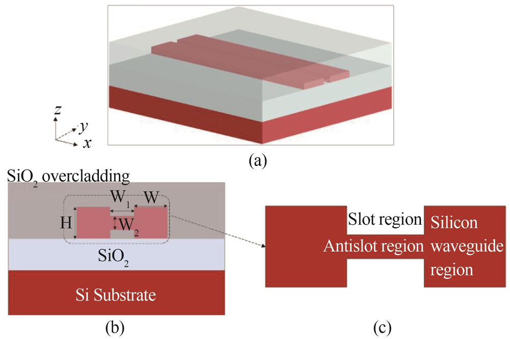
The three-dimensional (3D)structural diagram and the cross-section of the antislot waveguide are shown in Figs. 1(a-b),respectively. We studied the influence of structural parameters on mode confinement by the finite element method (FEM)at λ = 1 550 nm,as shown in Fig. 2(a). In the normalized mode area Aeff /A0,is the diffraction-limited mode area and Aeff is mode area given by[7]
,
where W()is the electromagnetic energy density given by Eq. 1. The refractive index of silicon and silica at the wavelength of 1 550 nm is 3.476 and 1.444,respectively. A normalized mode area of 3.4×10⁻² is achieved at W = 150 nm,W1 = 50 nm,and W2 = 20 nm,which is on the same order of magnitude as that of the plasmonic waveguides. The normalized electromagnetic energy density and electric vector distributions at these parameters are shown in Fig. 2(b). We can clearly see that electromagnetic energy is tightly confined in the nanoscale antislot region. The strong mode confinement is attributed to the electromagnetic orthogonal boundary conditions. As discussed in Sect. 2,because the electric vector [white arrows in Fig. 2(b)]is perpendicular to the interface of the slot and the silicon waveguide and the low-index slot region [Fig. 1(c)]is nanoscale in size,the electromagnetic energy density in the whole slot region is enhanced compared to that in the silicon waveguide region [Fig. 1(c)]according to the first boundary condition of electromagnetic field. Similarly,because the electric vector is parallel to the interface of the antislot and the slot and the size of the high-index antislot region [Fig. 1(c)]is also nanoscale,the electromagnetic energy density in the whole antislot region is greater than that in the slot region according to the second boundary condition. As shown by the white arrows in Fig. 2(b),the electric field is along with the y-direction which indicates the guided mode of the antislot waveguide is a quasi-TE mode. The quasi-TE mode is an eigenmode of the antislot waveguide and because the all-dielectric antislot waveguide does not contain metal,the quasi-TE eigenmode is theoretically lossless,which is consistent with our calculated results by the FEM,the negligible imaginary part of the effective refractive index. The theoretically lossless propagation of the all-dielectric antislot waveguide is a significant breakthrough compared with its plasmonic counterparts. Subwavelength mode confinement and theoretically lossless propagation can be achieved simultaneously in a single all-dielectric antislot waveguide,overcoming the trade-off between the two physical quantities.
Figure 1.(a)Three-dimensional structural diagram of the all-dielectric antislot waveguide,(b)its cross-section,(c)partial enlarged view of (b)Note:(a),(b),and (c)are all not drawn to scale
Figure 2.(a)Influence of structural parameters on normalized mode area of the all-dielectric antislot waveguide,(b)normalized electromagnetic energy density and electric vector distributions at W = 150 nm,W1 = 50 nm,and W2 = 20 nm. The definition of W,W1,and W2 is shown in Fig. 1(b)Note:The height of the waveguide is 220 nm
2.2 Coupling between the antislot waveguide and input/output fiber
A lot of applications can be achieved when light is confined in deep subwavelength scale,but due to the serious mode mismatch,the direct coupling between the input/output fiber and the small-size antislot waveguide is usually inefficient. Here,we proposed an efficient coupling scheme to improve the coupling efficiency. The whole light coupling structure is given by Fig. 3. The light from a fiber couples to a silicon waveguide through a conventional inverse taper firstly,then it transmits from the silicon waveguide to the antislot waveguide through an adiabatic linear taper coupler whose size gradually changes from that of the silicon waveguide to that of the antislot waveguide. The fiber used here is a lensed fiber with a 2.9 μm mode-field diameter (MFD)[33]. The height,width,and length of the silicon waveguide are 220 nm,350 nm,and 2 μm,respectively. The inverse taper has an 80 nm wide tip[33] and is embedded in a polymer waveguide. The polymer waveguide has a cross section of 3 μm×3 μm which is matched to that of the lensed fiber. The structural parameters of the antislot waveguide used here are the same as above. The refractive index of the polymer is 1.5 at λ = 1 550 nm and other material parameters are the same as above. We firstly optimized the position of the lensed fiber by calculating the overlap between the fiber mode and the fundamental TE mode of the polymer waveguide using the finite difference eigenmode (FDE)solver in commercial software Lumerical MODE. An optimal 94.6% (0.24 dB)overlap is achieved at y = 0 and z = 1.4 μm,and the misalignment tolerance for 1 dB loss penalty is about 2 μm in both y and z directions (Fig. 4). Then,we optimized the length of the inverse taper and the adiabatic linear taper using the eigenmode expansion (EME)solver in MODE for improving the coupling efficiency further. Figures 5(a-b)show the coupling efficiency from the lensed fiber to the silicon waveguide with the lensed fiber at the optimal position and from the silicon waveguide to the antislot waveguide,respectively. The coupling efficiency from the lensed fiber to the silicon waveguide increases along with the length of the inverse taper firstly and then tends to be stable. A coupling efficiency of 92.8% is achieved at a length of 150 μm,which includes the overlap loss of the fiber and the polymer waveguide. The coupling efficiency from the silicon waveguide to the antislot waveguide is very high even when the adiabatic linear taper is very short. A coupling efficiency of 97.7% is attained even without the adiabatic linear taper and it can reach up to 99.9% when the adiabatic linear taper is 8 μm. The adiabatic linear taper is mainly used to reduce the reflection from the silicon waveguide to the antislot waveguide caused by structural change abruptly,thus reducing the wave oscillation back and forth and avoiding the interference of incident wave and reflected wave. The electromagnetic energy transfer process from the silicon waveguide to the antislot waveguide is shown in Fig. 6,where (a)and (b)correspond to the case when the length of the adiabatic linear taper is 8 μm,(c)and (d)are the case of without the adiabatic linear taper. Clearly,the electromagnetic energy can be effectively coupled to the nanoscale antislot region of the antislot waveguide in the two cases. However,there are standing waves in the silicon waveguide in the case of without the adiabatic linear taper,which agrees well with the above statement. An overall coupling efficiency of 92.7% from the lensed fiber to the small-size antislot waveguide is achieved with 150 μm inverse taper and 8 μm adiabatic linear taper. This corresponds to an overall coupling loss of 0.33 dB.
Figure 3.(a)The light coupling structure from the lensed fiber to the antislot waveguide or vice versa,(b)partial enlarged view of (a)Note:(a)and (b)are both not drawn to scale. The zero in y and z directions is located at the middle of the coupling structure and the middle of the top silicon,respectively
Figure 4.Influence of the lensed fiber position on coupling efficiency and loss in (a)z and (b)y directions. The optimal fiber position in z and y directions is approximately located at 1.4 μm and 0,respectively
Figure 5.Coupling efficiency (a)from the lensed fiber to the silicon waveguide as a function of the inverse taper length (L1)with the lensed fiber at the optimal position and (b)from the silicon waveguide to the antislot waveguide as a function of the adiabatic linear taper length (L2)
Figure 6.Electromagnetic energy transfer process from the silicon waveguide to the antislot waveguide (a),(c)at the xz section with y = 0,(b),(d)at the xy section with z = 0 Note:(a)and (b)correspond to the case when the length of the adiabatic linear taper is 8 μm,(c)and (d)are the case of without the adiabatic linear taper
The whole electromagnetic energy transfer process from the antislot waveguide to the output end is shown in Fig. 7(a),where the length of the antislot waveguide,the adiabatic linear taper,the silicon waveguide and the inverse taper is 4 μm,8 μm,2 μm and 10 μm,respectively. To save simulation time,the length of the inverse taper here is set to 10 μm only to qualitatively exhibit the electromagnetic energy transfer process. The electromagnetic energy can be effectively coupled from the antislot waveguide to the output end. To illustrate the role of the adiabatic linear taper,Fig. 7(b)demonstrates the coupling process from the antislot waveguide to the output end without the adiabatic linear taper. Clearly,there is macroscopic reflection at the interface of the antislot waveguide and the silicon waveguide in the case of without the adiabatic linear taper,which further indicates the adiabatic linear taper can be used to reduce the reflection and avoid the interference of incident wave and reflected wave,mentioned above.
Figure 7.Electromagnetic energy transfer process from the antislot waveguide to the output end (a)the length of the antislot waveguide,the adiabatic linear taper,the silicon waveguide and the inverse taper is 4 μm,8 μm,2 μm and 10 μm,respectively,(b)corresponds to the case of without the adiabatic linear taper
We have demonstrated an all-dielectric antislot waveguide which can confine light into nanoscale antislot region. A normalized mode area of 3.4×10⁻² is achieved at the wavelength of 1 550 nm,which is on the same order of magnitude as that of the plasmonic waveguides. The strong mode confinement results from the electromagnetic orthogonal boundary conditions. Because the all-dielectric antislot waveguide does not contain metal,its supported quasi-TE eigenmode can propagate without loss in theory,which is a significant breakthrough compared with its plasmonic counterparts. The proposed all-dielectric antislot waveguide realizes subwavelength mode confinement and theoretically lossless propagation simultaneously,conquering the trade-off between the two physical quantities. On the other hand,a high-efficiency coupling scheme between the small-size antislot waveguide and the input/output fiber has also been proposed. The overall coupling efficiency of 92.7% can be obtained with 150 μm inverse taper and 8 μm adiabatic linear taper. The misalignment tolerance for 1 dB loss penalty is about 2 μm in both y and z directions. The excellent properties make the antislot waveguide have great application potential in many fields,such as increasing the integration density of photonic integrated circuits[34],improving the sensitivity of photonic sensing[35],and enhancing the fluorescence signals in bioimaging[36].